
All content Copyright 2022 Parallel Systems Ltd.
1. Select File>Open>Project.
2. Navigate to the C:\OrCAD_Training\Capture\DAAmp directory, and open the DAAmp.opj file.
3. Double-click on the .\daamp.dsn file to expand its contents.
(Observe that the list of schematic folders in this design includes a schematic folder labelled “DAAMP Circuit”)
4. Left-click on the DAAMP Circuit folder to select it
5. Select Edit>Copy from the top menu, or right-click>Copy.
6. Select the Project Manager window for the Training project.
7. Left-click on the .\training.dsn entry in this Project Manager window.
8. Select Edit>Paste from the top menu, or right-click>Paste
9. Save the Training design.
10. Close the DAAmp.opj Project Manager window. (Do not save it.)
11. Double-click on DAAMP Circuit folder just added.
12. Double-click PAGE1 in the DAAMP Circuit folder.
13. Zoom to all.
Observe that this schematic contains hierarchical port symbols which will match the pins of a hierarchical block in the referring schematic.
14. Close the schematic window.
15. Double-click on Data Schematic to expand the folder contents.
16. Double-click PAGE1 in the Data Schematic folder.
17. Zoom to all
18. Left-click the Place hierarchical block icon.
The Place Hierarchical Block window opens. Use this window to define the schematic that the hierarchical block represents.
19. In the Reference field, enter:
DAAMP1
20. Choose Schematic View from the Implementation Type drop-down.
21. Choose DAAMP Circuit from the Implementation Name drop-down.
Note
Since the DAAMP Circuit was copied into the Training project, leave the Path and filename field blank. This is referred to as an internal reference. If the DAAMP Circuit was not copied into the Training project, you would use the Path and filename field to specify the location of the release.dsn file. This is referred to as an external reference.
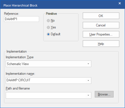
22. Left-click>OK.
You are now ready to draw the rectangle for a hierarchical block.
23. To the right of one of the 74ACT574 parts, left-click and drag a rectangle for the hierarchical block.
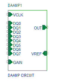
The block automatically contains hierarchical pins for each of the ports in the underlying DAAMP Circuit schematic.
24. Press Esc to deselect the hierarchical block.
25. Zoom in to see the block symbol.
If necessary, the following steps can be used to change the hierarchical block: To change the size of the rectangle, left-click on the DAAMP1 symbol and drag one of the corners to a new location, press Esc to deselect the block afterwards. To move a pin, left-click on the pin to select it and then hold the left-click down and drag the pin around the boundary of the hierarchical block.
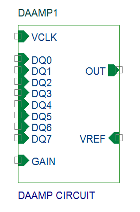
26. Arrange the pins, as shown in the following graphic.
27. Left-click on the DAAMP1 block to select it and right-click>Copy.
28. Press Esc to deselect and right-click>Paste.
A copy of the block symbol attaches to your cursor.
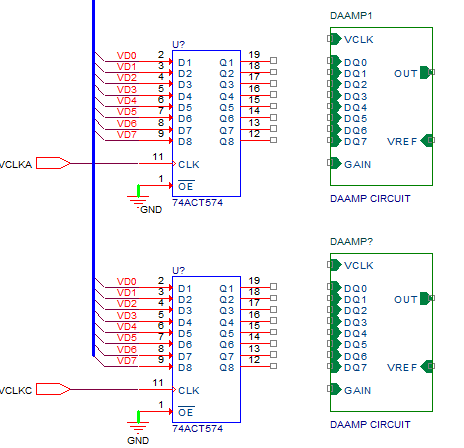
29. Left-click to place the copy to the right of the other 74ACT574 part, as shown in the following graphic.
30. Right-click>Edit Properties on the block just placed, set the Reference property value to DAAMP2.
(DAAMP2 will be underlined as a result of user assignment of the reference)
31. Press Esc to deselect.
Observe how the pins on the 74ACT574 line up with the pins on the hierarchical block.
Note
To avoid two occurrences of the DAAMP1 hierarchical blocks, Capture automatically names the second hierarchical block DAAMP2 when the Automatically reference placed parts option is checked in the Options>Preferences, Miscellaneous tab. Make sure this is NOT selected for this exercise.
32. From the Project Manager window, open PAGE2 of the Release Root Schematic.
33. Left-click the DATA Schematic block located in the bottom centre portion of the page.
34. With the DATA block highlighted, right-click>Synchronize Down
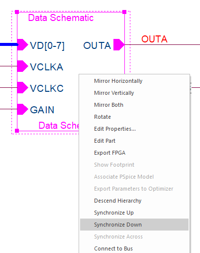
The lower level schematic opens. The new ports OUTA and OUTB are located on the right hand side of the page and GAIN is located on the left hand side of the page. (If necessary, press F5 to get the schematic page view refreshed.)
Note
The Synchronize Down command could also be used to verify the links from a block symbol to it’s referenced schematic. If nothing additional appears on the referenced schematic page, all links are present and up to date. If hierarchical ports appear on, or are removed from, the schematic page, the block and referenced schematic were not synchronised.
35. Move the added ports nearer to the DAAMP1 and DAAMP2 block symbols as shown in the following graphic. (If you want, rotate the port symbols through 360 degrees to get the text “tight” to the port symbol)
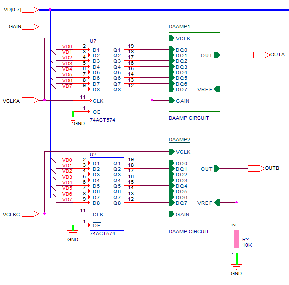
36. Add connections from the DAAMP1 and DAAMP2 blocks to each of the 74ACT574 parts.
Note
A quick way to do this is to move a block symbol so that its pins touch the pins of a 74ACT574, then “drop” the block, check that you have 8 “red dots” for the connection changes to create connections between the overlapping pins, then move the block symbol to the right and observe that wires are automatically added between the part and the block.
A portion of Data Schematic PAGE1 is shown above, use this example as a guide to help you follow lab instructions and complete the schematic.
37. Add wires to hierarchical ports OUTA and OUTB of both blocks.
38. Add wires from the GAIN input port to the GAIN pin of DAAMP1 and DAAMP2 as shown in the graphic at the beginning of this lab section.
39. Connect one VCLK pin on DAAMP1 to the VCLKA and one VCLK pin from DAAMP2 to VCLKC hierarchical port.
40. Copy a Resistor from the “terminator group” to the right of the page to near the lower right corner of DAAMP2, this will have all of the required properties.
OR:
Place a RESISTOR from the Design Cache (in Place>Part), right-click and select Edit Properties to set its Value to 10K and its PCB Footprint to SM_0805, to near the lower right corner of DAAMP2.
41. Connect one end of the resistor to the VREF pins on both blocks.
42. Copy a GND symbol and connect it to the other end of the resistor.
43. Save the design.
End of Lab
All content Copyright 2022 Parallel Systems Ltd.