
All content Copyright 2022 Parallel Systems Ltd.
1. Select File>New.
The New Drawing dialog box appears.
2. Type the following name in the Drawing Name field:
samtec_sqt-120-01-f-d
3. Select Package Symbol from the scrolling list of drawing types, as shown below
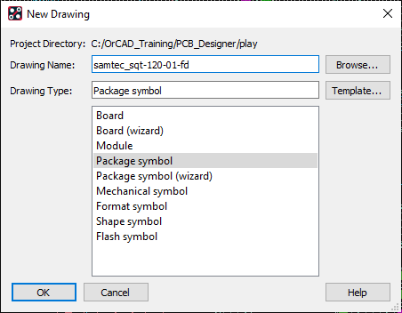
4. Check that the Project Directory is still “play”, left-click>OK to close the New Drawing dialog.
5. Left-click>OK on the “Create a new design” form
6. Select Setup>Design Parameters.
7. Check / modify the Design tab parameters as required to match the following values:
Type: Package
User Units: Millimeter
Size: A4
Accuracy: 2
Left X: -50
Lower Y: -50
(OK any messages about change of accuracy)
8. Left-click>OK.
9. Select Layout>Pins from the top menu.
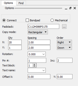
The Options window displays fields for adding pins.
10. In Options, left-click the “…” button next to the field for Padstack.
A padstack browser appears.
11. Choose the padstack c112h086ps170 from the list
12. Left-click>OK to accept the padstack name.
The PCB Editor Command Window states:
Using ‘c112h086ps170.pad’
13. Move the mouse to Options and set the options for the pins as follows:
X to Qty 20, Spacing 2.0, Order Right
Pin # 1, Inc 2
TextBlock 1
Offset X / Y 0.0
14. To place the pins, left-click in the Command Window and type the following:
x 0 0
(Ensure that you use lower case x <space> 0 <space> 0)
15. Press Enter.
(20 pins are placed numbered 1, 3, 5 and so on)
16. Move the mouse back to Options and set:
Pin # 2 and keep Inc 2 and the other settings
17. Left-click in the Command Window and type the following:
x 0 2
(Again, ensure that you use lower case x <space> 0 <space> 2)
18. Press Enter.
19. Move the mouse to the canvas background and right-click>Done to end placing pins.
20. Select Setup>Areas>Package Boundary from the top menu
21. Move the mouse to the PCB Editor Command Window and left-click at the prompt, then type in the following commands:
x -1.15 -1
iy 4
ix 40.3
iy -4
Press Enter after each command
(Remember to use lowercase characters for the commands)
22. Move the mouse to the canvas background and right-click>Done to end adding the boundary.
23. Select Setup>Areas>Package Height from the top menu
24. Move the mouse to the canvas and left-click to select the Package Boundary just created
25. Move the mouse to Options and set the Package Height Max to 6.35 (mm)
26. Move the mouse to the canvas background and right-click>Done to set the package height
27. Select Setup>Grids from the top menu
28. Set the Non-Etch grids to X: 0.05, Y: 0.05
(These fine grids are required to trace the Package Boundary, these are not strictly required to be set at this point since an alternative method to using mouse clicks will be employed to add the lines for the details)
29. Left-click>OK to set the grids
30. Select Add>Line from the top menu
31. Move the mouse to Options and Check / Set the Active Class and Subclass to PACKAGE GEOMETRY / ASSEMBLY_TOP
32. Move the mouse to the lower left corner of the Package Boundary outline, hover the mouse over the corner intersection and right-click>Snap Pick To>Segment Vertex
33. Move the mouse to the other corners, “up and across”, or “across and up”, and use right-click>Snap Pick To>Segment Vertex at them in turn to define the Assembly outline.
34. Once the Assembly outline has been defined, right-click>Next
35. Move the mouse to Options and change the subclass to SILKSCREEN_TOP and set the Line Width to 0.25 (mm)
36. Move the mouse back to one of the corners of the Package Boundary and repeat the process of right-click>Snap Pick To>Segment Vertex for each of the corners to add the Silkscreen outline.
37. Once the Silkscreen outline has been defined, right-click>Next
38. Move the mouse to the Lower Left corner of the package and add a 45 degree line at that corner.
(Exactly where this is added is not too important, the purpose is to define a “marker” to indicate Pin 1 of the package. Check that Options has Line lock of 45 for this)
39. Right-click>Done once the marker has been added.
(The grids were set to draw the outline with mouse clicks but the “Snap pick to” method was used since the fine grid would require rather careful picks)
40. Select Layout>Labels>RefDes from the top menu
41. Move the mouse to Options:
Check / Set the Active Class and Subclass: REFDES / ASSEMBLY_TOP
Text Block 4
42. Move the mouse to the “middle” of the Package Boundary and left-click to set the text position, exactly where this is placed is not critical
43. Type:
J*
as the RefDes placeholder value
44. Right-click>Next
45. Move the mouse back to Options and set the Active Subclass:
SILKSCREEN_TOP
46. Move the mouse back to the “middle” of the Package Boundary, this time move above the text just added and left-click outside of the Package Boundary to set the text position, again exactly where is not critical.
47. Type:
J*
as the RefDes placeholder value
48. Right-click>Done to end adding RefDes
49. Select File>Save from the top menu
(The file samtec_sqt-120-01-f-d.dra gets saved to disk, the contents are checked and then the file samtec_sqt-120-01-f-d.psm gets created if the checks pass)
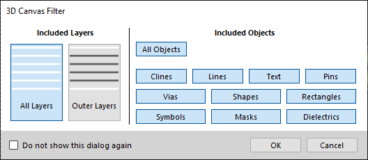
50. Select View>3D Canvas from the top menu
51. Check that “All Objects” is enabled for the 3D Canvas filter that is displayed and left-click>OK to open the 3D Canvas.
52. At the upper right of the 3D Canvas, select the 3D Mapper tab. (If the 3D Mapper tab isn’t shown, check the settings under View>Windows and enable the 3D Mapper entry with a left-click)
53. In the 3D Mapper tab, left-click the “…” button to the right of Model File and browse to the step folder in the play folder.
(Full path is C:\OrCAD_Training\PCB_Designer\play\step)
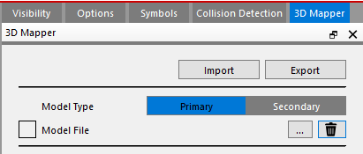
54. Select Samtec-SQT-120-01-f-d.step from the folder and left-click>OK
55. When the step file is loaded you will see that the orientation isn’t correct.
(The connector model is “laid on” the board, rather than going through it)
56. In the 3D Mapper tab, left-click the AUTO button.
(This will attempt to automatically map the step model)
57. Auto gets the step model aligned to go through the board but the step model “body” remains above the board surface. Press and hold the Shift key and press and hold the middle mouse button (wheel) and the cursor will change to a “hand”, move the mouse to rotate the view so that the Pins can be seen at the bottom of the step model.
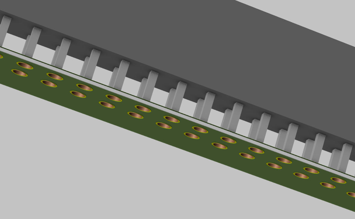
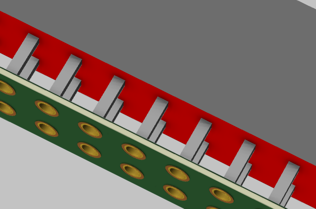
58. Left-click the TOP button in the 3D Mapper tab, then move the mouse to the step model in the canvas and to the bottom face of the step model (where the pins are). The face will turn red when the mouse is over it, then left-click to get the bottom face of the step model mapped to Top of the board.
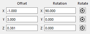
The final mapping parameters will be:
59. Select File>Close to close the 3D Canvas. The mapping will be saved to the DRA file when File>Save is used from the PCB Editor window.
End of lab
All content Copyright 2022 Parallel Systems Ltd.