
All content Copyright 2022 Parallel Systems Ltd.
1. Select File>New from the top menu.
2. Type the following name in the Drawing Name field:
soic16
3. Select Package Symbol from the scrolling list of drawing types, as shown below:
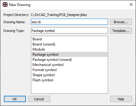
4. Check the Project Directory is set to “play” and left-click>OK to close the New Drawing dialog box.
5. Left-click>OK on the “Create a new design” form
6. Select Setup>Design Parameters from the top menu.
7. Select the Design tab and check:
Units: Mils (change to Mils, if required)
Size: A
Accuracy: 2 (Decimal places)
Left X: -500
Lower Y: -1500
8. Choose the Display tab.
9. Left-click the Setup Grids browser button.
10. In the Non-Etch section at the top of the form:
a. Double-click in the Spacing: x: field and type: 25
b. Double-click in the Spacing: y: field and type: 25
11. Left-click>OK at the bottom of the Setup Grids form.
12. Left-click>OK to close the Design Parameter Editor form.
13. Select Layout>Pins from the top menu.
14. In Options, select the “…” button next to the empty field for Padstack.
15. Select the padstack r193_060mr218_086 (scroll through the list, or use r193* for the filter).
16. Left-click>OK to close the padstack browser
The PCB Editor command window states:
Using ‘r193_060mr218_086.pad’
17. To add pins 1 through 8 in a row, in Options, verify the spacing and order match below, double-click in the Qty field for the Y direction, and enter: 8 and set the spacing to 50
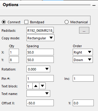
18. Press Tab.
19. Move the mouse to the PCB Editor command window and left-click in it, then type:
x 0 0
20. Press Enter
21. Move the mouse back to the canvas and Zoom in to the area surrounding the pins you just placed.
22. Move the mouse back to Options and set the Y order field to Up.
23. To set the pin number text to the right of the respective pins, double-click in the Offset X: field and enter:
50
24. Press Tab.
25. Move the mouse to the PCB Editor command window and left-click in it, then type:
x 225 -350
26. Press Enter.
27. Move the mouse to the canvas background and right-click>Done to exit the Add Pin command.
Next the Assembly and Silkscreen outlines will be added to get to the following:
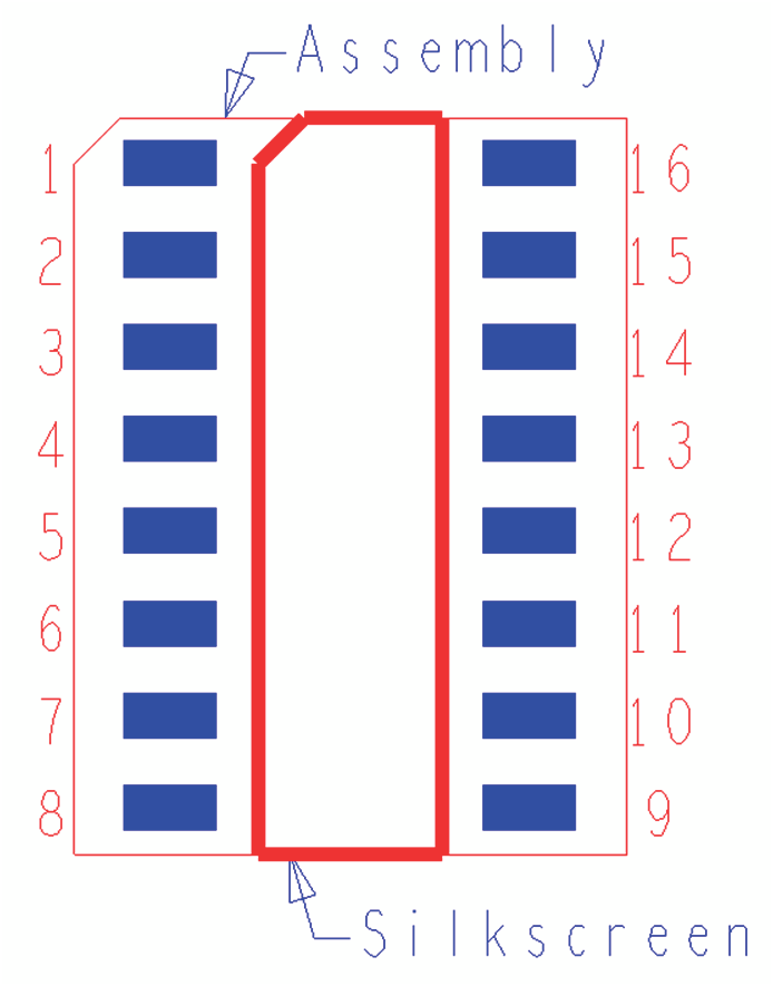
28. Select Add>Line from the top menu.
29. Move the mouse to Options and Check / Set the Active Class and Subclass:
PACKAGE GEOMETRY / ASSEMBLY_TOP
30. Move the mouse to the canvas and use left-clicks to draw the corners of the outline.
31. Once the Assembly outline has been added, right-click>Next to move on to adding the Silkscreen outline
32. Move the mouse to Options and change the Active Subclass to:
SILKSCREEN_TOP
(Set the Line Width in Options as well to override the “zero” width)
33. Move the mouse back to the canvas and use left-clicks to define the Silkscreen details
34. Right-click>Done to end the Add Line command
35. Select Layout>Labels>RefDes from the top menu.
36. Move the mouse to Options, change the Rotate field to 90, and change the Text Block field to 2.
37. Left-click inside the device (within the silkscreen outline) to define a location for the text.
38. In the PCB Editor command window, type:
U*
39. Right-click>Done from the pop-up menu to end the Label command.
40. Select Layout>Labels>Device from the top menu.
41. Left-click inside the device (near the refdes label) to place the start of the text
42. On the keyboard, type:
devtype
43. Right-click>Done from the pop-up menu to end the Label command.
44. Select Layout>Labels>RefDes from the top menu.
45. Move the mouse to Options, change the Active Subclass to SILKSCREEN_TOP and set the rotation back to 0
46. Left-click outside the assembly outline to set a text location
47. In the PCB Editor command window type:
U*
48. Right-click>Done from the pop-up menu to end the Label command.
(The finished symbol should now resemble the screenshot below)
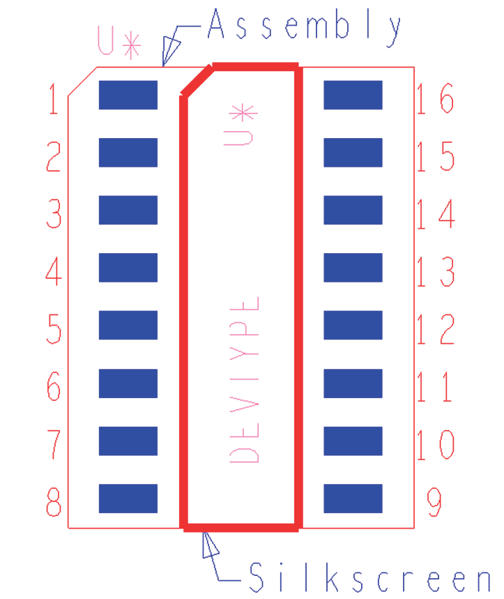
49. Select File>Save from the top menu.
PCB Editor saves an soic16.dra file, checks the file and creates a soic16.psm if the checks pass.

End of Lab
All content Copyright 2022 Parallel Systems Ltd.