
All content Copyright 2022 Parallel Systems Ltd.
1. Start OrCAD Capture, or OrCAD Capture CIS from:
Start (Windows Icon) >Cadence PCB 17.4-2019>Capture CIS 17.4
Select any OrCAD Capture, or OrCAD PCB Designer, license if you see the License Picker.
(Which license / product is selected is not important for this exercise)
2. Use File>Open>Project and browse to the C:\OrCAD_Training\PCB_Designer\project directory, select the Release.opj file and Open.
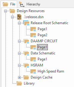
3. If necessary, open the “+” symbols for Design Resources, Release.dsn and DAAMP Circuit so that the Project Window display resembles the following screenshot:
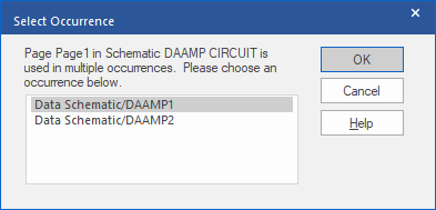
4. Double-click on the Page1 Schematic Page entry in the DAAMP CIRCUIT Schematic Folder, you will be prompted for one of the Occurrences, select the Data Schematic/DAAMP1 entry and OK.
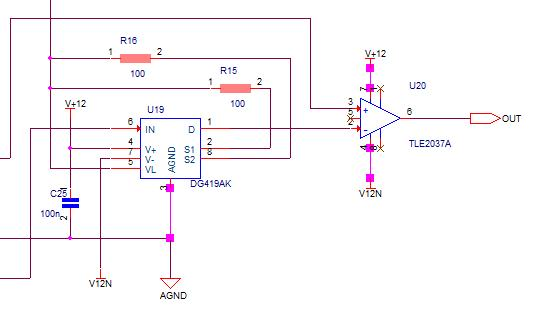
5. Select the AGND, V+12 and V12N wires (not the power symbols or symbol names) as shown below: (left-click on the first net and then control+left-click to select the next two).
6. With the nets selected, right-click>Edit Properties.
7. In the Property Editor, change the “Filter by” to Capture PCB Editor. (or any of the PCB filters)
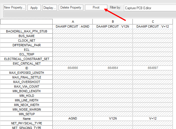
Left-click the Pivot button to change the orientation of the Properties listing.
8. Left-click in the NET_PHYSICAL_TYPE cell and drag the mouse to the NET_SPACING_TYPE cell to select all the cells for both properties, then right-click>Edit
(Or left-click on the first named cell and control+left-click on the second named cell to select both)
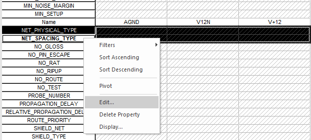
9. Set the value of the property to POWER for both cells and left-click>OK to close the popup.
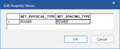
The property sheet should now look like this:
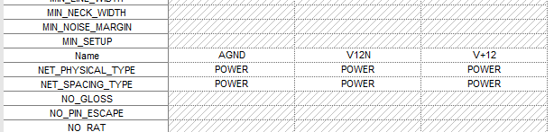
(The Property Values are not case sensitive, they will be converted to Upper Case in the Logic data)
10. Right-click>Close on the Property Editor tab, or use the “X” on the tab, Yes / OK any changes if prompted.
11. Right-click>Close on the Data Schematic tab, Yes / OK any changes if prompted.
12. Select PCB>Design Sync Setup from the menu and check the settings.
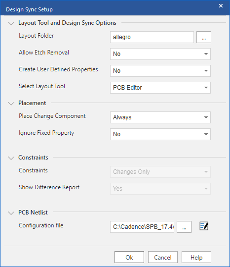
13 . Left-click>OK to close the Design Sync Setup form.
14. Select PCB>New Layout from the main menu.
Use the “…” button to browse to the “master.brd” previously created in the C:\OrCAD_Training\PCB_Designer\project folder.
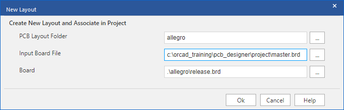
15. Left-click>OK to create the new “release.brd” in the allegro sub-folder.
16. When the Cadence Product Choices window appears, select an OrCAD PCB Designer Standard or Professional license entry from the list.
17. Close OrCAD Capture
(This step is not absolutely essential but the PCB and Schematic tools will have Intertool Communication enabled and this will have some impact on outright performance. Cross-probing will be looked at later in the course)
18. In PCB Editor, select Place>Components Manually and notice that your reference designators appear in a list when the Components by refdes option is active.
19. Left-click>Close to close the Placement window.
20. Select File>Save As from the top menu.
A file browser window opens.
21. In the File Name field, enter:
unplaced
22. Left-click>Save to save the unplaced.brd file in the project\allegro directory.
(All the board related output will be written to the project\allegro directory from now on)
23. At this point you can either exit from the PCB Editor program by selecting File>Exit, or you can leave this design open, ready to begin lab exercises for the next lesson.
If you exit from PCB Editor at this point in the lab, when you restart PCB Editor it will automatically open the unplaced.brd file from the C:\OrCAD\PCB_Designer\project\allegro directory.

End of Lab
All content Copyright 2022 Parallel Systems Ltd.