
All content Copyright 2022 Parallel Systems Ltd.
Work through Labs 7-1 to 7-3 to use the Constraint Manager in PCB Editor, or skip to Labs 7-1a to 7-3a to use the Constraint Manager in Capture.
1. Start PCB Editor, if it’s not already running.
2. Choose File>Open and open the unplaced.brd design file you saved previously, if it is not currently open.
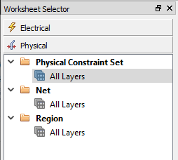
3. Select Setup>Constraints from the PCB Editor main menu.
The Constraint Manager opens, select the Physical domain on the left hand side.
4. Select the All Layers Worksheet under the Physical Constraint Set folder.
This should be the worksheet already open, but it is good practice to make sure you have the correct worksheet open.
5. In the Default row, left-click in the Min Line Width and Min Neck Width cells and change the values to 0.15, as in the following graphic:
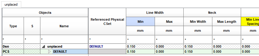
(Take care not to select the entire Default row as all of the values will be edited)
6. Left-click the Default cell to select the entire row.
7. Select Objects>Create>Physical CSet from the Constraint Manager menu. (Or right-click>Create>Physical CSet in the Default cell)
8. In the Create Physical CSet form, type Clocks and left-click>OK
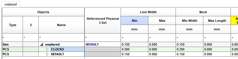
9. In the Clocks row, left-click in the Min Line Width and Min Neck Width cells and change the values to 0.2 as in the following screenshot:
10. Left-click the Clocks cell and right-click>Create>Physical CSet.
11. Name the new Physical CSet Power
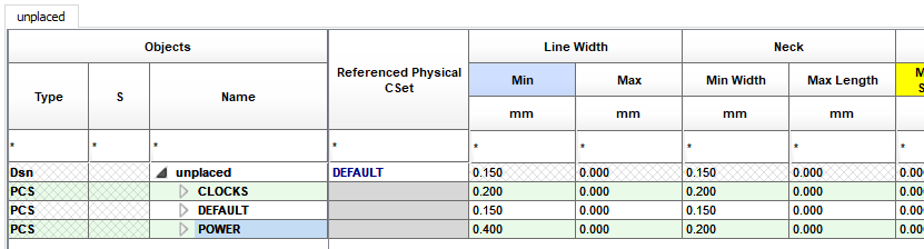
12. In the POWER row, left-click in the Min Line Width cell, change the value to 0.4
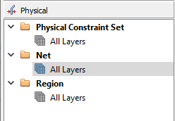
13. Select the All Layers worksheet under the Net folder as shown below.
14. Scroll down through the list of nets section so that both the VCLKA and VCLKC nets are visible.
15. Left-click to select the VCLKA net, and shift+left-click the VCLKC net so that both nets are selected, or drag-select the two net names.
16. Right-click>Create>Class from the pop-up menu.
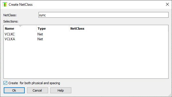
17. Enter the name SYNC in the Net Class field. Verify that the “Create for both physical and spacing” option is checked, and left-click>OK.
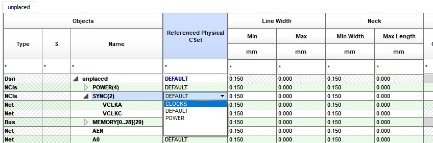
18. Scroll back to the top of the list of Nets and see that the SYNC class has been created with two members, VCLKA and VCLKC, select the Referenced Physical CSet cell in the SYNC row and select Clocks from the pull-down menu as shown.
19. The NET_PHYSICAL_TYPE properties that were added to the schematic in the previous session lab caused the creation of a POWER net class in the board file. Go to the cell for the Referenced Physical CSet for the POWER Net Class and select the POWER Physical CSet from the drop-down.
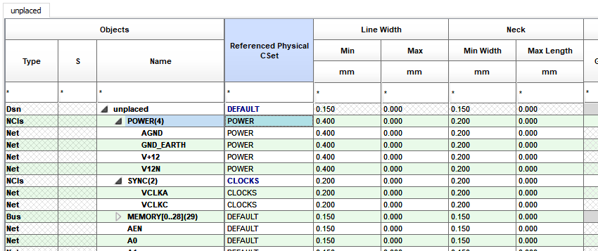
(this image has the Net Classes “opened” to show the CSet assignment to the individual members of the Net Classes.)
20. Select File>Close from the Constraint Manager window.
21. Select File>Save As. from the top menu in the PCB Editor window.
22. Rename this drawing by entering the following in the File Name field:
constraints
23. Left-click>Save to save the constraints.brd file.
The constraints.brd file is saved to disk.
Do not exit from PCB Editor. The next lab will continue from this point.
End of Lab
All content Copyright 2022 Parallel Systems Ltd.