
Component Placement is possibly the most important stage in PCB design since poor placement will almost always result in a design with any reasonable complexity being a lot more difficult to connect that it might be with good placement. The placement of some components, like terminators close to a driver, may be determined by signal quality requirements.
As far as can be achieved, placing components so that the ratsnests that indicate the connections from the netlist are as straight as possible is usually something to aim for. This isn’t always possible so, the resulting placement is usually a compromise that gives the most “straight line” ratsnests that can be managed.
Components are placed on the “non-Etch” grid, defined in Setup>Grids. The placement grid will always be a compromise, too fine and operations like aligning components could be more difficult than it might be, too coarse and it might not be possible to place the design within the Design Outline.
When PCB Editor starts after loading the netlist, there are no components placed in the design canvas. Whilst moving a small number of components around on the canvas might be productive in a small design, this isn’t appropriate for larger designs. If required, components can be placed on the canvas with the Quickplace command.
Components, Package Symbols, can be removed from the canvas but they will remain as part of the design as “unplaced”. To permanently remove a component from the design requires an updated netlist.
Mechanical and Format Symbols which are not part of the netlist can be placed through the Place menu. Deleting Mechanical and Format Symbols which are not part of the netlist will permanently remove them from the design.
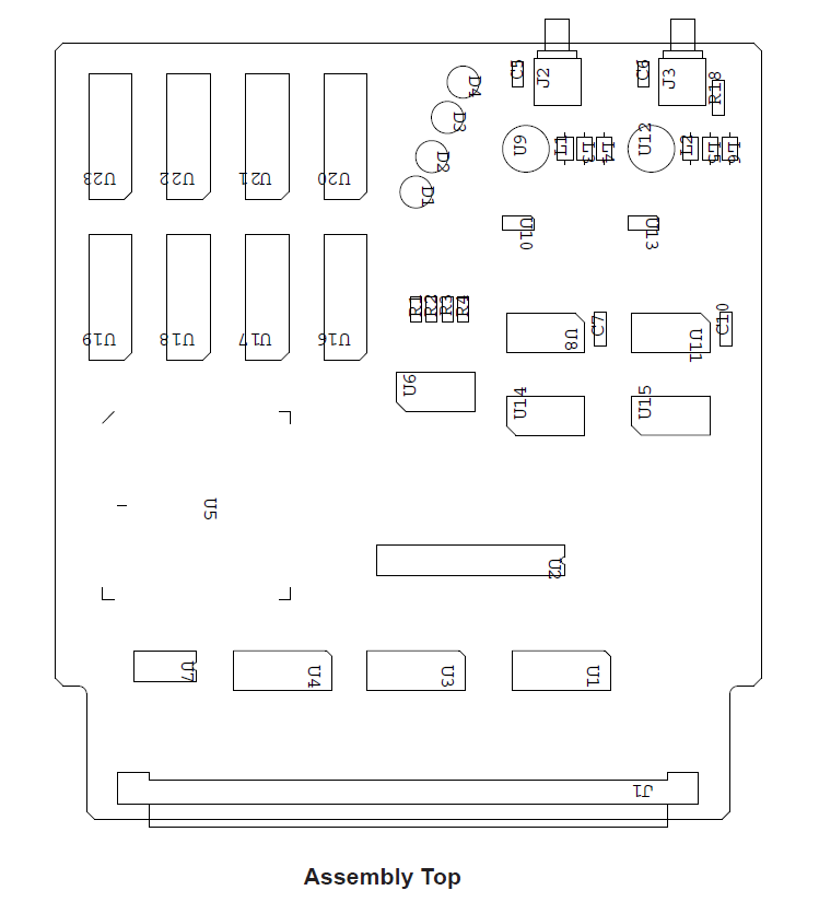
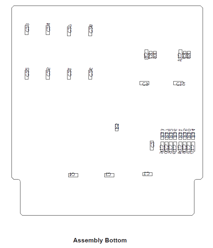
The following two images show the suggested final placement for the lab design. Try to get the ratsnest lines as straight as practical, especially for the eight sets of resistor / capacitor terminators. This design isn’t difficult to place and placement on both sides of the board is not essential to getting the components placed but it is useful to practice. Note that the resistor and capacitor footprints used in this design have Route Keepouts to prevent routing between the Pins. Also note that components will be correctly placed in the Room by the Quickplace function, this may not match all of the screen shots but the components should not be moved outside of their assigned Rooms, there will be DRCs if this is the case.
All content Copyright 2022 Parallel Systems Ltd.