
All content Copyright 2022 Parallel Systems Ltd.
1. Be sure you are working on the board file partplaced.brd. It is the board we saved in the previous lab.
2. Choose Display>Zoom>World to display the entire extents of the drawing.
3. If the grids are displayed, turn them off by left-clicking the Grid Toggle icon. 
4. Choose Place>Quickplace from the top menu.
The Quickplace form is displayed. Change the settings as shown:
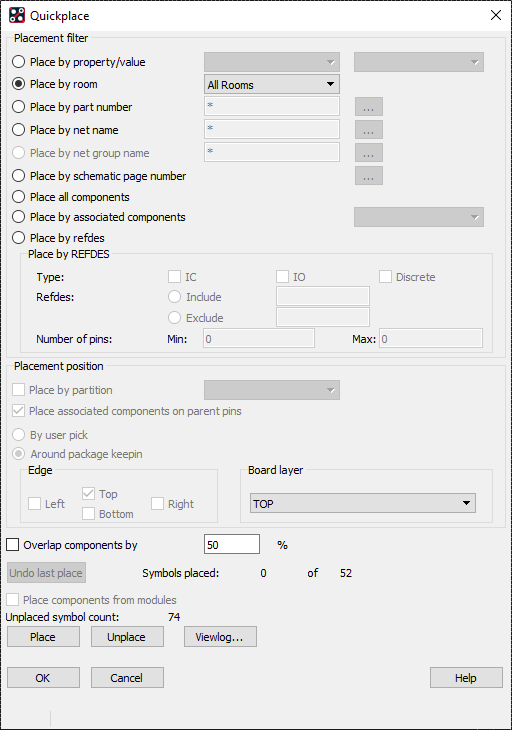
(Place by Room: All rooms, Board layer: Top)
Notice that you selected All Rooms to be placed, this will place each component with a Room property and place it in its appropriate room on the Top side of the board,
5. Left-click>Place, this places all the parts with Room assignments.
6. Left-click>OK to close the Quickplace form.
7. You can use the Mirror, Move, Group Move, and Rotate commands to rearrange the locations and orientation of the Symbols as needed.
Be sure to set Colours to have visibility ON for the following:
Package Geometry: Assembly_Top, Assembly_Bottom, Place_Bound_Top, Place_Bound_Bottom; Components / Ref Des: Assembly_Top Assembly_Bottom
It may also help to have different colours for the Top and Bottom for the subclasses.
8. The final placement location is up to you.
You may want to use Setup>Application Mode>Placement Edit, then right-click in the canvas and set Super Filter to Symbols (Or set the Find for only Symbols) during placement. In Placement Edit Application Mode, left-click on a Symbol will attach it to the cursor to move, the next left-click will place. You may also want to take a look at the Dynamic Alignment Guides, Setup>User Preferences, Display, Align Guides, Enable Dynamic Alignment.
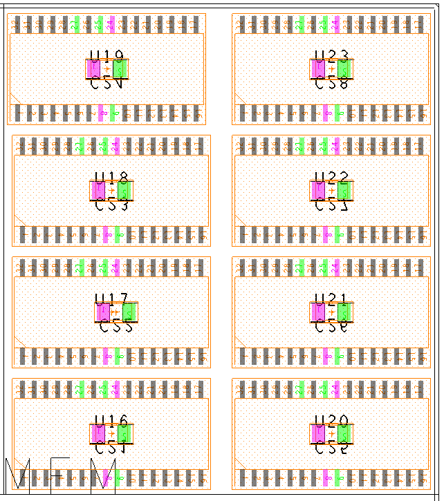
Here is a placement suggestion for the MEM room:
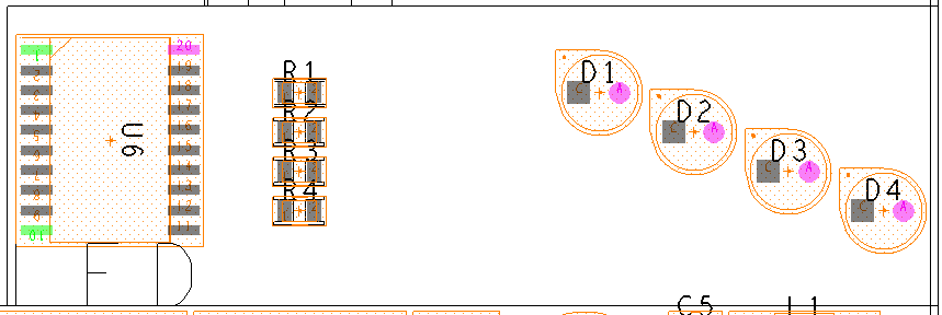
Here is a placement suggestion for the LED room:
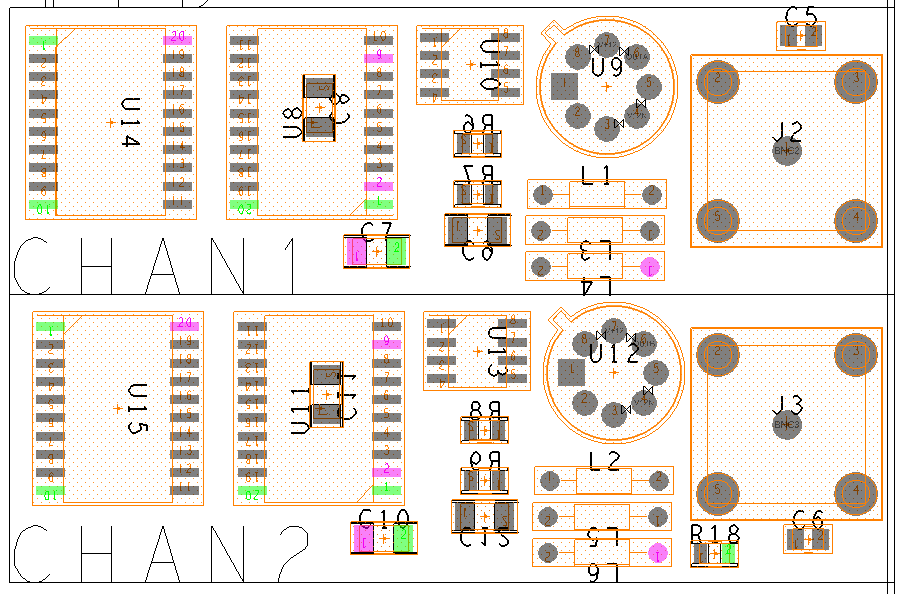
Here is a placement suggestion for the CHAN1 and CHAN2 rooms:
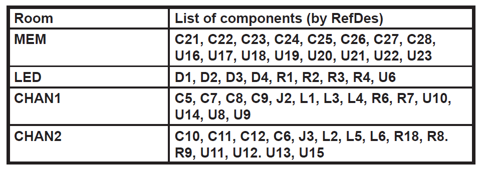
Below is a table of the rooms defined and the parts that should be placed in each room:
9. Select File>Save from the top menu to save the partplaced.brd file. (OK to overwrite)
10. Choose Display>Zoom>World to display the entire extents of the drawing.
11. Select Place>Quickplace to display the quickplace form.
12. Toggle on Place by refdes. Be sure the Type IC is toggled.
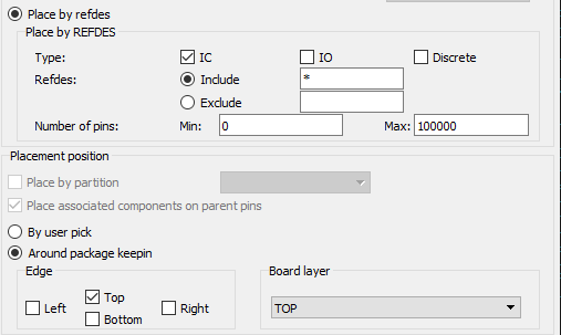
13. Left-click>Place at the bottom of the form.
The 8-pin dip is placed on the top edge of the board outline.
14. In that same form, change the Place by Refdes Type from IC to Discrete.
15. Toggle the Board Layer to Bottom and the Board Edge to Bottom.
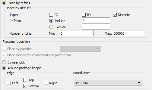
16. Left-click>Place at the bottom of the form.
17. Left-click>OK at the bottom of the form to close the Quickplace form.
18. Zoom in closer.
19. Relocate the placement of the capacitors and resistors that were just quickplaced to match the completed picture later in the lab. Use all the commands you have already practised (including Edit>Move, Edit>Rotate, Edit>Mirror, Place>Components Manually and Edit>Delete), to move the Symbols.
As an alternative, if you prefer, use the following instructions and flip-design to place the components.
Place C13 – C20 and R10 – R17 on the Bottom side of the PCB.
Get the components from the quickplace locations and roughly place them in the area shown. Then get the board view to roughly the same as the following picture.
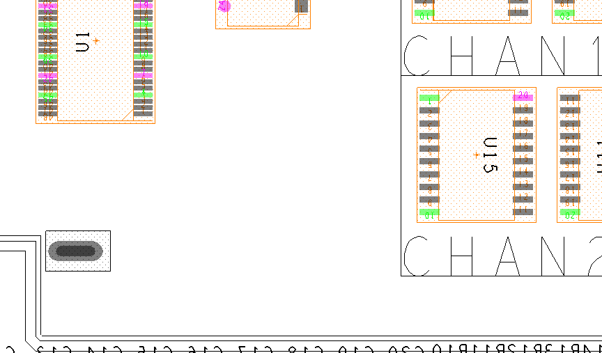
The components will be placed in the free area shown.
To view the board in flip-design mode, use Display>Flip Design from the menu.
The view of the board will now resemble the following picture:
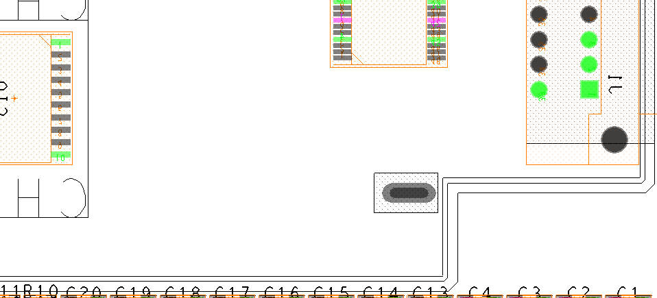
Now move the components as before while the design is flipped, note that the “bottom” refdes now displays correctly and the “top” refdes is reversed.
The completed section should resemble the following picture:
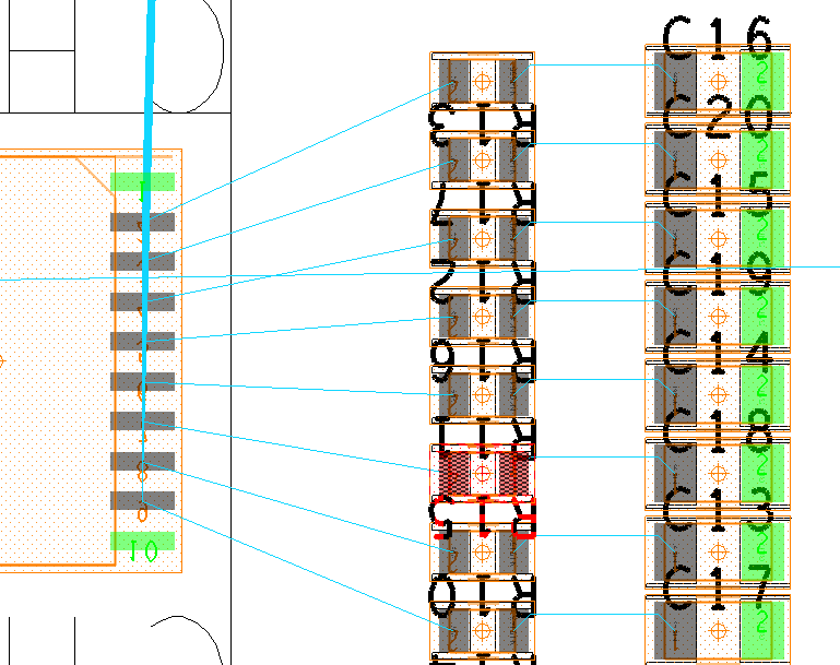
Use Display>Flip Design to get back to the “Top View”.
20. Use Display>Zoom>Fit to see the entire board.
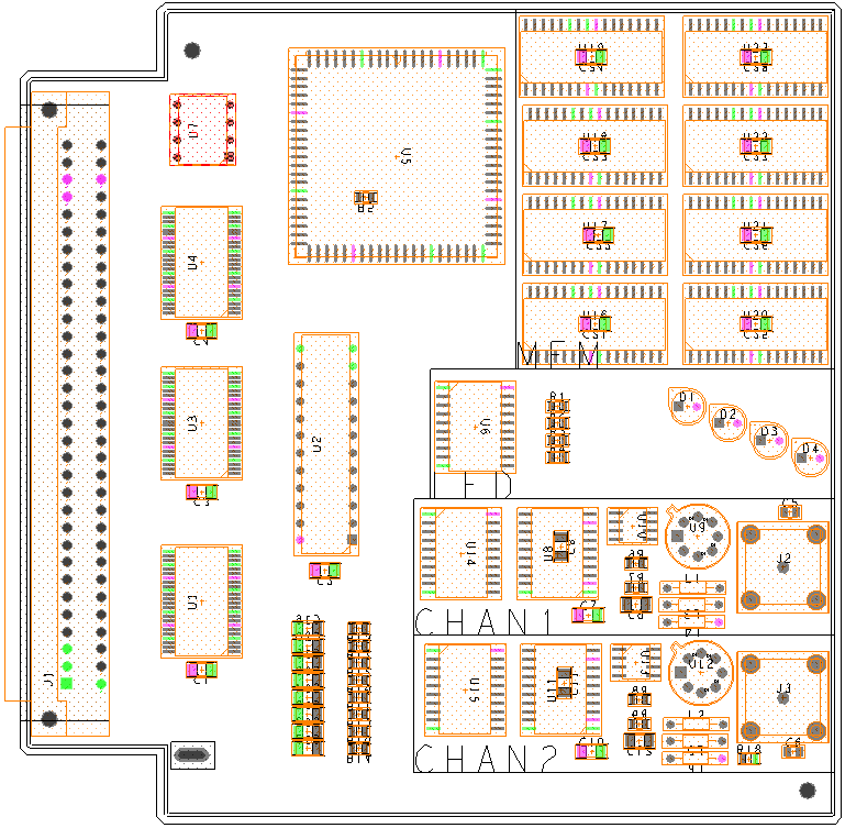
21. When you have completed manual placement, choose File>Save As from the top menu.
22. Rename this drawing by entering the following in the File Name field:
placed
23. Left-click>Save to save the placed.brd file.
24. To create a report of placed components, choose Export>Reports.
A Reports form appears.
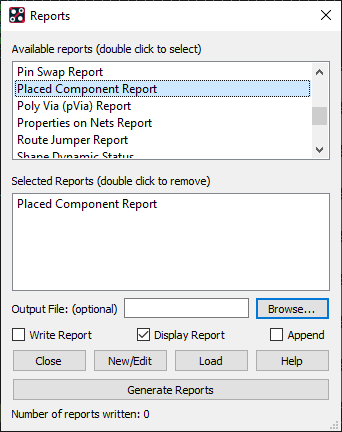
25. Use the scroll bar in the Report field to view all the available types of reports that you can generate.
26. Double-click the Placed Component Report. This sends the report name to the lower window. Then left-click>Generate Reports
A Report window appears with a list of all placed components. In this case, the report should show you have placed all 82 components.
27. Left-click the “X” icon, or use the upper right X to exit from the Report window.
28. Double-click on the Placed Component Report in the lower window if you want to create another report and don‘t want to see the Placed Component Report again.
29. To create a report of unplaced components, double-click the Unplaced Components Report from the scroll list to send that name to the lower window.
30. Left-click>Generate Reports
The Unplaced Component Report form appears. If there were any components that appeared in the Unplaced Components report, be sure to place them before continuing.
31. Exit from the Report window by left-clicking on the “X” icon.
32. Exit the Reports form by left-clicking on Close.
33. You can also use the Check>Design Status command to see if all parts are placed.
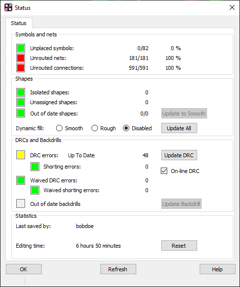
Oh! There are 48 errors, you may have some more, in which case the component placement needs to be checked, there are likely to be some Place Bounds touching other Place Bounds, or Room Outlines for example.
What are these 48 errors related to? The circular, 8-pin parts have pins closer than the 0.4mm Spacing Rule required by the Spacing CSet assigned to the Power Pins. Spacing DRCs get reported for each layer, 6 layers in the cross-section, 4 pins in error and 2 parts in the design for a total of 48 DRCs. The pins are 0.386mm apart so, in this case: the DRCs could be ignored, we will see waiving of DRCs in a later lesson; the Pad sizes could be changed, that will also be discussed in a later lesson; or a property could be added to let PCB Editor ignore the cause of these DRCs, as follows:
34. Select the U9 and U12 parts in the design canvas. If you set the Application Mode to Placement Edit, you will need to change the Application Mode back to General Edit for these steps. Set the Super Filter for Symbols, left-click on one of the circular, 8-pin, parts and control+left-click on the other.
35. With the mouse hovering over one of the selected circular, 8-pin, symbols, right-click>Property Edit.
36. Locate the Nodrc_Sym_Same_Pin entry in the Available Properties list and left-click on the entry to add the property.
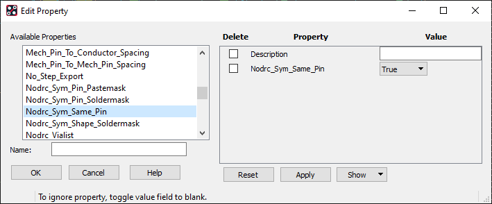
37. Left-click>OK to close the Edit Property dialog.
38. Use the Check>Design Status to verify that all of the DRCs have been removed before moving on from this lab since, whilst it will be possible to continue with DRCs, it may not be so easy to change the placement to remove placement related DRCs once the board has been routed.
39. Choose File>Save from the top menu, left-click>OK the message to overwrite the placed.brd file that was saved when the placement was completed. The updated placed.brd file is written to disk.
End of Lab
All content Copyright 2022 Parallel Systems Ltd.