
All content Copyright 2022 Parallel Systems Ltd.
Start PCB Editor from:
Start (Windows Icon) >Cadence PCB 17.4-2019>PCB Editor 17.4
The PCB Editor Canvas opens.
1. Select File>Open from the PCB Editor main menu.
2. If necessary, set the File Type for Board (*.brd)
3. Use the Browse button to navigate to the C:\OrCAD_Training\PCB_Designer_Advanced directory, select the backdrill_complete.brd file and left-click on Open.
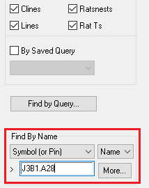
4. Zoom into the connector pin field using “Find By Name” in the Find Filter Tab
- Open the Find Tab
- Select Symbol(or Pin) from the Find By Name pull down
- Entering J3B1.A28 should centre and zoom the display to the pin.
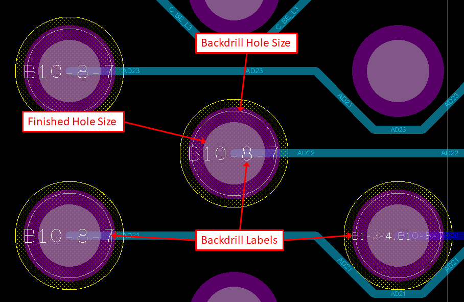
5. All backdrill sites will have special drill labels indicating the Backdrill Start Layer, To Layer and Must Not Cut Layer.
- Format: (B<Start Layer #>-<To Layer>-<Must Not Cut Layer>)
- When backdrill occurs on both sides of the board the backdrill label will specify details for both separated by a comma.
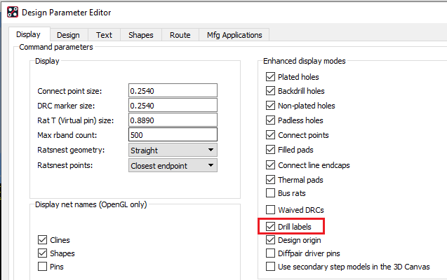
- Display of Backdrill Labels are controlled by enabling Drill Labels in Design Parameters Editor (Setup>Design Parameters) under the Display Tab.
6. Backdrill Hole Size will be displayed as a hollow circle to differentiate between Finished Hole Size which is a filled circle. Zoom out slightly so you can see the surrounding pins and change the Active
Subclass to BOTTOM under the Option Tab to see the view below.
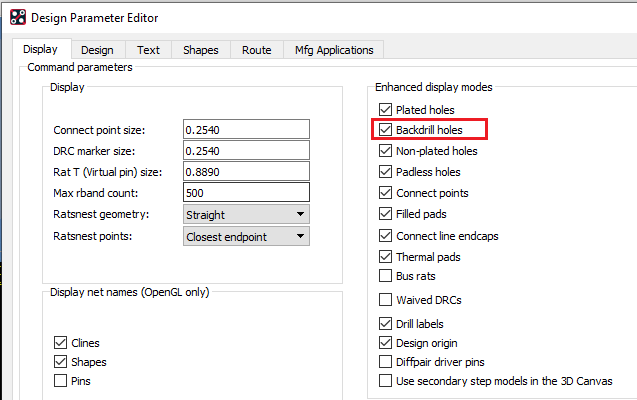
7. Display of Backdrill Hole Sizes are controlled by enabling Backdrill Holes in Design
Parameters (Setup>Design Parameters) under the Display Tab
8. Zoom into pin J3B1.A29 using Find By Name in the Find Filter tab.
9. Now step through the layers effected by the backdrill. Under the Visibility Tab, select the Global Visibility Off button to turn off all layers.
10. Notice that the Visibility Pane in this design has Soldermask and Pastemask Top and Bottom available for visibility selection.
11. Select Enable Layer Select Mode at the bottom of the Visibility tab to allow quick single click selection to display layers.
12. Select the hyperlink style text (underlined blue text) for Soldermask Top to turn on the SOLDERMASK_TOP subclasses.
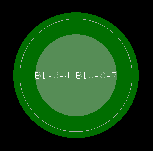
13. Notice the Soldermask pad geometry has been automatically updated based on the value entered in the Padstack Mask Tab under the BACKDRILL_SOLDERMASK Pad Geometry. The Soldermask opening should be larger than the Backdrill Hole Size.
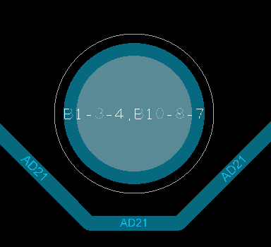
14. Select the hyperlink style text (underlined blue text) for Top to turn off all other layers and just turn on the TOP subclasses. Notice the Top pad geometry has been automatically updated based on the value entered in the Padstack Design Tab under BACKDRILL_START Regular Geometry. Reduction of the pad geometry on the backdrill start layer is required to prevent accidental plating at the backdrill site during fabrication.
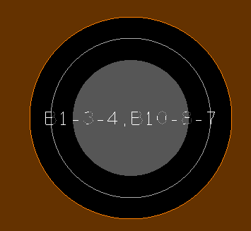
15. Select the hyperlink style text (underlined blue text) for Layer_2_P to turn off all other layers and just turn on the LAYER_2_P subclasses. Notice the Anti Pad geometry on the Negative Plane has been automatically updated based on the value entered in the Padstack Design Tab under BACKDRILL_CLEARANCE Anti Pad Geometry. Larger Anti Pad clearance required to clear Backdrill Hole Size
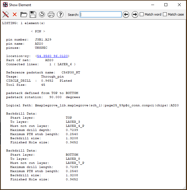
16. Hover over a Backdrilled Pin and right click>Show Element to review that Backdrill Data which is now available in the Show Element results window.
17. Save the board, overwriting the existing backdrill_complete.brd.

End of Lab
All content Copyright 2022 Parallel Systems Ltd.