
All content Copyright 2022 Parallel Systems Ltd.
Start PCB Editor from:
Start (Windows Icon) >Cadence PCB 17.4-2019>PCB Editor 17.4
The PCB Editor Canvas opens.
1. Select File>Open from the PCB Editor main menu.
2. If necessary, set the File Type for Board (*.brd)
3. Use the Browse button to navigate to the C:\OrCAD_Training\PCB_Designer_Advanced directory, select the viaarray.brd file and left-click on Open
4. From the menu take Place>Via Array and set the Options, as shown:
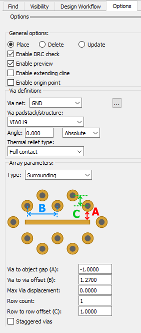
5. Select the board outline to choose the location of the via boundary.
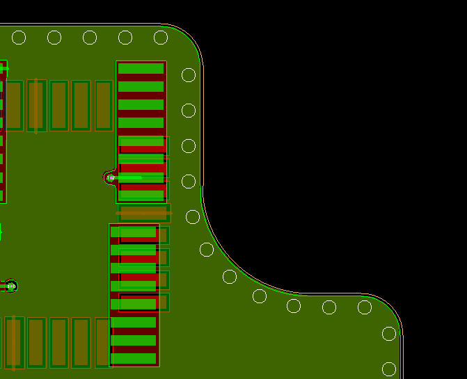
A preview of the vias is now shown. They can be placed with a left-click but if you want to make changes to the options you can, see next step.
6. Change the value of Via-object offset to 1.000mm notice how the display is dynamically updated.
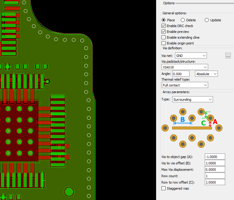
Note that any potential DRCs that might be generated are not flagged at this stage.
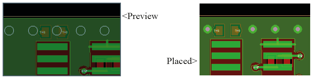
7. Left-click outside of the board to place the vias from the preview and, in this case, since the “Enable DRC Check” was set in Options when the Preview was generated, Vias that would have caused a DRC have been removed as the Via Array was placed.
8. Right-click>Done to complete the command.
9. Zoom into the area that is routed between U9 and U10, bottom of the PCB, right hand side. Turn off the Visibility for the Top Layer to see the route.
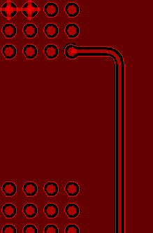
10. Select Place>Via Array and set the Options as follows:-
Enable DRC Check, Enable Preview, Via net = GND, Padstack = VIA019
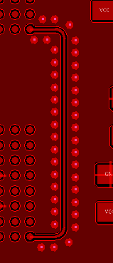
Array parameters: Type: Surrounding. Set the Via to object gap to 0.5mm.
11. Left-click on the Cline and see how the vias are positioned surrounding it.
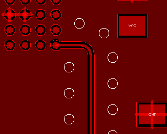
12. Once again, the view is dynamic so adjust the via-object offset to 0.2032mm and note how the preview updates to show the change in the distance to the cline.
13. Place the vias with right-click>Place
14. Hover over one of the vias located in the via array. (Either the one around the board edge or the one around the Cline) and right-click>Show Element
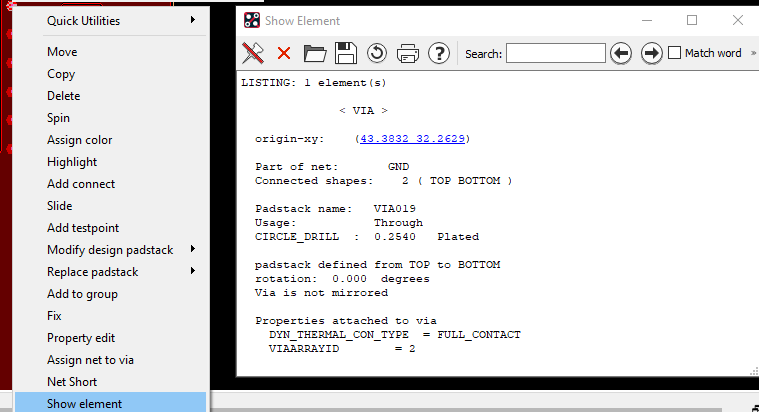
15. Note that the via has been set to full_contact based on the settings in the Options panel. At the same time it has been given a unique VIAARRAYID property which can be used to remove the via array if required.
16. Use either of the “cross” icons to close the Show Element window.
17. Select Place>Via Array. Change the Options pane setting from Place to Update. Change the Via to Via Offset from 1.0mm to 0.5mm The Preview is updated.
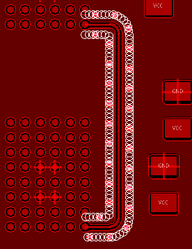
18. Right-click>Place to place the vias.
19. Select Place>Via Array. Change Options from Update to Delete
You can left-click on one of the vias that are part of the array you wish to remove and that array is deleted.
Note that you are dealing with Via Arrays rather than individual vias with this command, you can still delete individual vias with Edit>Delete without affecting other vias in the array.
20. Right-click>Place to accept the change.
There may be a requirement to cover the entire PCB with vias to stitch the planes together.
21.Go to the Options pane and set as follows:
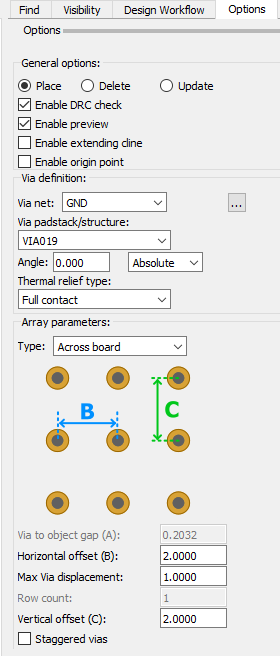
22. Left-click anywhere in the canvas to show a preview of the vias.
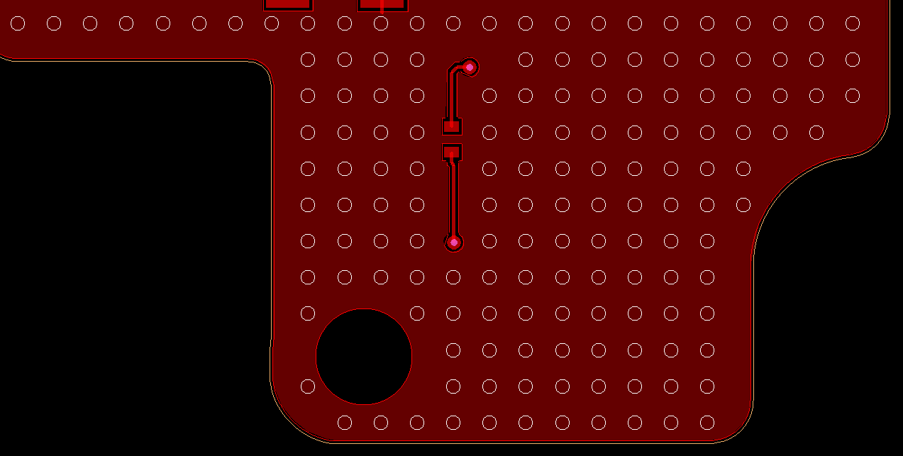
23. Right-click>Place to place the Via Array (if required)
24. Experiment with the settings as required, remember that the Via array will update dynamically as the settings are changed. Once you have the required settings, right-click>Place to place the vias. Note again that any vias that would cause DRCs are automatically deleted.
25. Right-click>Done to finish.

End of Lab
All content Copyright 2022 Parallel Systems Ltd.