
In this lab we will cover the Electrical Rules that can be setup for OrCAD PCB Professional or higher. These are typically used for high-speed memory (DDR), sophisticated serial interfaces (USB), and more complex constraints (timing, impedance) creating new design challenges.
Examples of high-speed memory might require complex constraints such as:
Relative Propagation Delay for the Data byte lane
x-mm between all members (including pin and z-axis delay)
Relative Propagation Delay for Address / Command / Control
x-mm between Controller and T-Point
x-mm between memory ICs and T-Point
Min/Max Propagation Delay
x-mm between Memory ICs and termination resistors
Differential Static and Dynamic Phase Tolerance
x-mm for all Data Strobe and Clock Differential Pairs
The series of labs covers:-
Net Scheduling
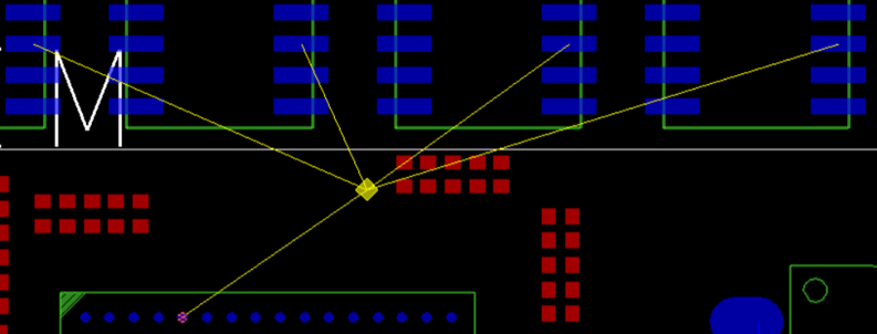
This allows nets to be defined for a specific routing path or pattern. T-points are virtual points which define a location point that nets, or segments will start/end.
Single Ended Impedance
Users can enter a value of required Impedance into Constraint Manager then the routed thickness is calculated based on a BEM2D field solver, The key to this calculation is an accurate Cross Section definition including thickness, dielectric constant and Conductivity.
Min/Max Propagation Delay
This manages delay in terms of length, % Manhattan length pin pairs. The DRC responds to both routed and unrouted conditions allowing users to evaluate timing rules at the component placement stage.
Relative Propagation Delay
Manage delay of matched groups between objects of different nets in terms of length or percent of Manhattan length. There are two options:-
Relative Delay – Delta:Tolerance (0:0.5mm) assigns a ‘target’ to the object with the longest Manhattan length and can be reassigned if necessary. Members must meet this value within the delta and tolerance specified.
Match Delay – :Tolerance (:0.5mm) matches members within tolerance only, no target.
Z Axis and Pin Delay
Electrons don’t just travel from pin to pin on single layers. They can travel in the z-axis through vias and pins as well as inside the package from die to pin. For high speed designs with delay rules, every piece (length) of copper needs to be included or you could be facing length mismatches which will cause performance issues. Now users can use a 2d field solver in combination with your stackup to calculate precise propagation and Z-axis length.
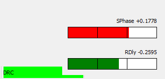
Electrical Constraint Heads up display
Gives users real-time heads-up constraint display which provides direct feedback while tuning and editing high speed constrained nets as a guide to compliance. Shown on nets that have Total Etch Length, Static and Dynamic Phase Tolerance (Diff Pairs) and Propagation Delays (Relative and Min/Max).
Differential Pair Static and Dynamic Phase Control
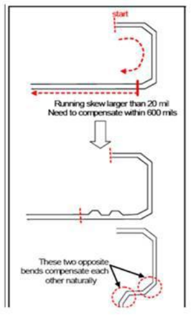
Static Phase controls the matched length of differential pair, checked over entire net from driver to receiver.
Dynamic Phase is checked based on a max length and tolerance from driver to receiver. The Dynamic Phase check is designed to meet the guidelines that suggest that the path lengths within the differential pair must differ by no more than “x mm” along the entire path of the net. If at any point on the net, the skew between them exceeds “x mm”, this mismatch needs to be compensated within “y mm”.
Total Etch Length
A mode which allows an minimum and maximum value to be set for the entire length of a net (excluding z axis). Routing lengths must meet within the minimum and maximum values specified.
All content Copyright 2022 Parallel Systems Ltd.