
All content Copyright 2022 Parallel Systems Ltd.
This example design is a cut-down version of a DDR memory design that only has:-
four address signals DDR3_A0-3
four data signals DDR3_DQ0-3
a differential strobe signal DDR3_DQS0_N and _P.
A single mode signal DDR3_DM0.
Only the “rats” for these nets are enabled.
Start PCB Editor from:
Start (Windows Icon) >Cadence PCB 17.4-2019>PCB Editor 17.4
The PCB Editor Canvas opens.
1. Select File>Open from the PCB Editor main menu.
2. If necessary, set the File Type for Board (*.brd)
3. Use the Browse button to navigate to the C:\OrCAD_Training\PCB_Designer_Advanced directory, select the schedule.brd file and left-click on Open
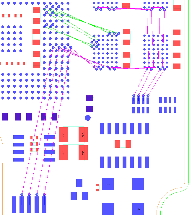
4. From the menu, Edit>Net Schedule
5. Start by left clicking on a Pin with a purple rat on J1, then U5 and then on the corresponding pin on U7, then U8, U9 and U10. The pins that can be selected are highlighted. After left clicking the pin on U10 finish with the pin on RN1 and then right-click>Done Note that this will end the Net Schedule command.
6. Repeat the process for the remaining three address signals, you can use right-click>Finish to end scheduling the current net and pick another net to schedule, rather than start Net Schedule for each net, right-click>Done when the four address nets have been scheduled.
Your result will look similar to the following screenshot:
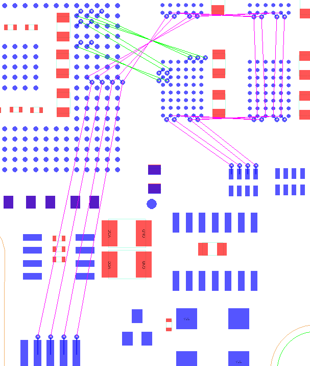
The nets are now scheduled in a clockwise direction around the pins from the connector to the resistor network.
7. Launch Constraint Manager using Setup>Constraints, or use the “CM” icon, and go to Electrical domain / Net / Routing / Wiring.
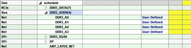
8. To verify that all the address signals are scheduled. Unfold the Bus DDR3_ADDR, left-click on the “triangle” next to the name, and make sure that the Schedule column is User Defined for all 4 address signals.
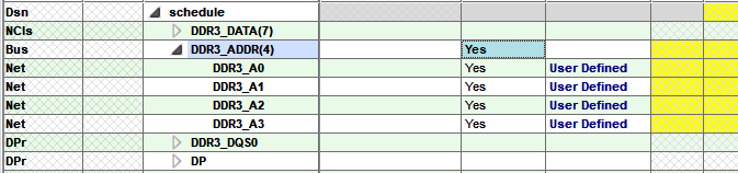
9. PCB Editor can verify that when the nets are routed they meet the schedule as defined, to enable this set Verify Schedule = Yes for DDR3_A0-3. You can either do this for each individual net or with one click by changing the cell for the bus. A left-click in the cell will get a drop-down to select the “Yes” option.
10. Also add a Stub Length / Max value of 0.762mm, again this can be added to individual nets, or to the nets as a group. Without this constraint the net must be routed from pin to pin without any kind of sharing. In this example the connections will share a fanout via instead of having 2 fanout vias per pin or 2 connections going to the pin. So it will be from via to via with a stub allowed to each pin.
11. You’ll notice that once the value is added the columns for Actual and Margin for stub length remain Yellow (along with the Schedule values). This is because the DRC modes are not enabled. You can enable these modes through Analyze>Analysis Modes / Electrical Modes and turn on the Stub length / Net schedule check or you can right-click the column header “Schedule” or “Max” (both Yellow) and check Analysis mode.
12. That completes this section. Save this board file, File>Save As and set the filename to schedule_save.brd

End of Lab
All content Copyright 2022 Parallel Systems Ltd.