
All content Copyright 2022 Parallel Systems Ltd.
Start PCB Editor from:
Start (Windows Icon) >Cadence PCB 17.4-2019>PCB Editor 17.4
The PCB Editor Canvas opens.
1. Select File>Open from the PCB Editor main menu.
2. If necessary, set the File Type for Board (*.brd)
3. Use the Browse button to navigate to the C:\OrCAD_Training\PCB_Designer_Advanced directory, select the schedule_prop.brd file and left-click on Open
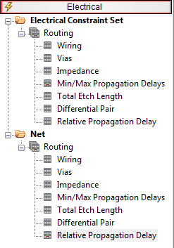
4. Open Constraint Manager and go to Electrical>Net>Routing>Relative Propagation Delay worksheet
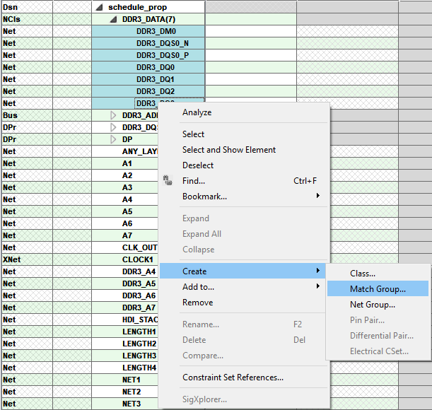
5. Expand the Netclass DDR3_DATA and select the nets DDR3_DQ0-3, DDR3_DM0, DDR3_DQS0_N and DDR3_DQS0_P within it and right-click>Create>Match Group
6. In the Create Match Group window specify the name for the match group as bytelane0 and click OK. By default the Match Group (MGrp) is added at the top.
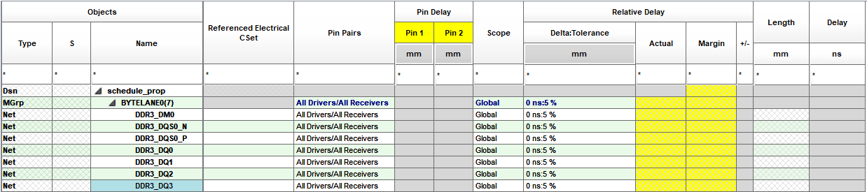
7. In this case the tolerance must be 0.5mm so change the Delta:Tolerance value for BYTELANE0 to 0mm:0.5mm, just typing 0:0.5 in the cell will get the design units added.
Now all signals within the match group must have equal length within +/- 0.5mm. This means that the maximum length difference between the longest and the shortest signal can be 1.0mm.
8. At this point, you can expand the BYTELANE0 group and right-click>Analyze in the BYTELANE0(7) cell, the Length column will then contain the routed stub lengths, about 1.0mm in each case.
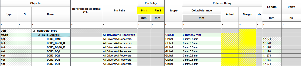
9. It is also possible to get Constraint Manager to check, DRC, the Unrouted lengths, use Analyze>Analysis Modes, Electrical, Electrical Options and check the two boxes in the DRC Unrouted group and OK the change, now go back to the BYTELANE0 group and right-click>Analyze again (if required), now you will see a Resulting Pin Pair, RePP, which will report the Manhattan Length, orthogonal X / Y distance for the unrouted portion and a Target picked for the longest Manhattan Length value.
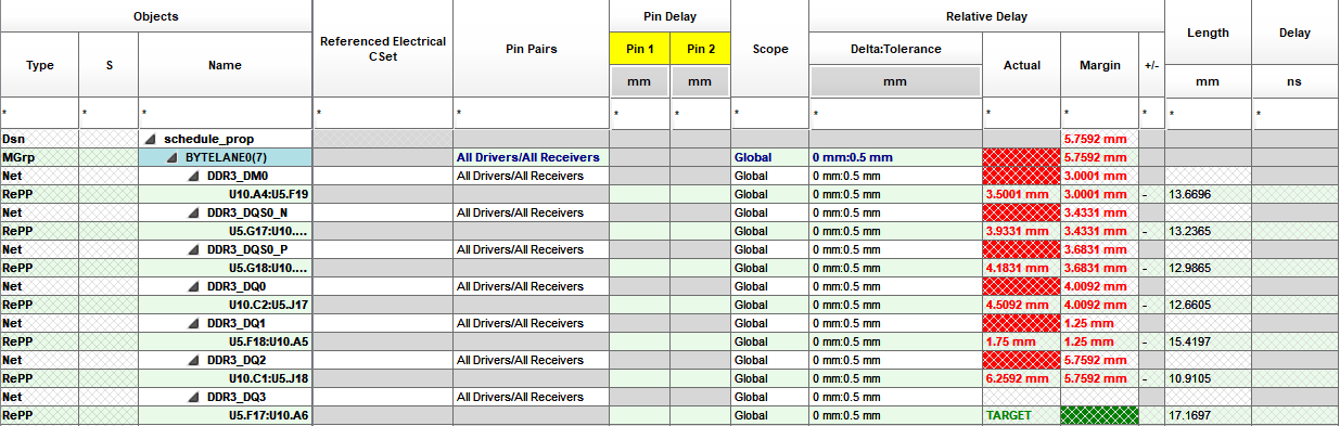
10. Go to PCB Editor and route the remaining connections for the nets in the Match Group BYTELANE0. Tip – These are the green rats.
11. Switch back to Constraint Manager and Select BYTELANE0 and right-click>Analyze. Now that the nets are routed, the Length column will reflect the routed lengths in all cases, Net and RePP.
It is usually good practice to change the target to the net with the longest routed length. After the signals are routed the constraint manager can easily help identifying the longest signal. If the longest signal is target then all other signals must be tuned with extra length which usually is much easier than shortening signals.
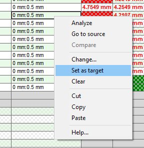
12. Double-click the column named Length to sort the Length column values. In this case, the longest Manhattan Length also has the longest routed length, if your routing has a different longest routed length, use right-click>Set as Target in the Delta:Tolerance cell for the Net to change the Target.
13. Switch back to the PCB Editor canvas and tune the signal lengths in the Match Group using Route>Delay Tune for the nets other than the Target.
Note: If the ‘Target’ is one of the signals in the diff pair and there is a DRC error on the diff pair then it will be necessary to delay tune using Right-click>Single Trace mode depending on the pattern used for delay tuning.
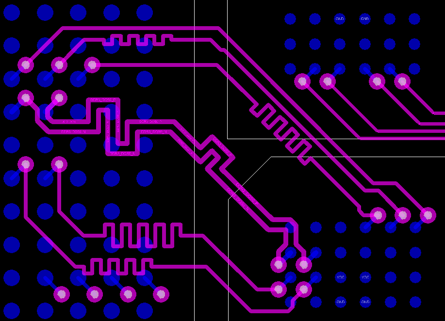
14. After using the Delay Tune to match the nets, switch to the Constraint Manager and verify the results. (The lack of DRC markers in the PCB Editor canvas will also confirm that the rules have been met.)
Schedule Prop Relative Propagation Delay for Pin Pairs
The previous part of this exercise just used “All drivers/all receivers” because the bytelane members were simply point-to-point connections. In this next part we will go through the setup for a more advanced match delay constraint. The signals DDR3_A0-A3 must be matched for the length from U5<>U10. This can be setup easily through the use of pin-pairs. Specifying a pin-pair directly from U5>U10 will work since the net schedule already specifies how the net should be routed.
15. In Constraint Manager open the Electrical>Net>Routing>Relative Propagation Delay worksheet.
16. Expand the Bus DDR3_ADDR, select the net DDR3_A0 and right-click>Create>Pin Pair
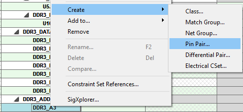
17. In the Create Pin Pairs dialog select U5.M21 and U10.H2 and click OK to create the pin pair.
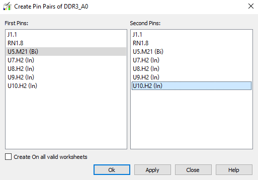
Accept the warning about unused Pin Pairs being removed when the Constraint Manager is closed. Just be aware of this also being the case for your own designs.
18. Repeat the steps above to create pins pairs for DDR3_A1-A3 between U5 and U10.
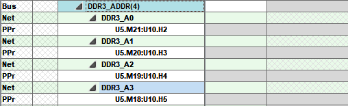
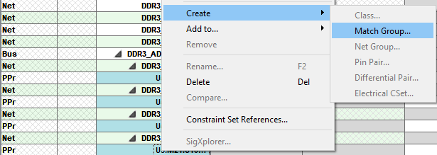
19. Select the 4 pin pairs just created with control+left-click, then right-click over one of the entries and take Create>Match Group
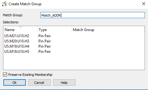
20. Name the Match Group Match_ADDR in the Create Match Group dialog and click OK.
21. Locate the Match Group in the worksheet and Set the Delta:Tolerance to 0mm:0.5mm, if required select the match group name and right-click>Analyze to show the values for the match group.

22. Switch back to the PCB Editor canvas and use Delay tune to adjust the length for the connections between U5 and U10 that are too short.
Since the constraint is set for the pin-pair U5<>U10 it does not matter if the adjustment takes place on the connection between U5<>U7, U7<>U8, U8<>U9 or U9<>U10. Try this out and tune the signals so they met the required relative propagation delay constraints.

24. Save the Board as schedule_match.brd
For more information on match groups please refer to the application note here:-
https://www.parallel-systems.co.uk/wp-content/uploads/2020/02/Match_groups.pdf

End of Lab
All content Copyright 2022 Parallel Systems Ltd.