
All content Copyright 2022 Parallel Systems Ltd.
Start PCB Editor from:
Start (Windows Icon) >Cadence PCB 17.4-2019>PCB Editor 17.4
The PCB Editor Canvas opens.
1. Select File>Open from the PCB Editor main menu.
2. If necessary, set the File Type for Board (*.brd)
3. Use the Browse button to navigate to the C:\OrCAD_Training\PCB_Designer_Advanced directory, select the vision.brd file and left-click on Open
4. Use Display>Vision Manager to open the Vision Manager to select the Vision mode.
5. From the drop-down, select Route Vision with a left-click.
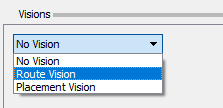
6. Left-click>Configure to select which routing checks to perform.
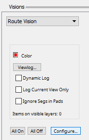
7. Set the option for: “Non-Optimised Segs”, “Non-Ideal Pad Entry”, “90 Degree Corners” and “Min Miter / Corner Size” As shown in the following screen shot.
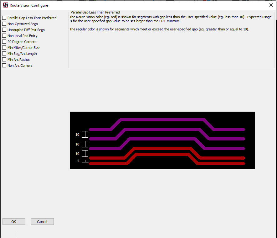
8. Then left-click>OK. The Vision Manager form will show some options related to the checks that have been configured, the check boxes can be used to toggle the visibility of the particular routing violation category in the canvas. You can also change the Channel Air Gap and Min Corner Size if required. Any violations will have a default colour of red. (This can be changed by right clicking the coloured swatch, then choose the colour you want with a left click).Hover the mouse over the displayed violation to get a datatip describing what the violation is.
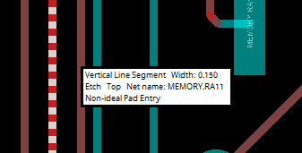
Note that, while the Route Vision is enabled, and changes made to the routing will cause the Route Vision to be updated. The Route Vision can be removed by setting the Visions drop-down to “No Vision” and the Visions form closed with the “X”.

End of Lab
All content Copyright 2022 Parallel Systems Ltd.