
All content Copyright 2022 Parallel Systems Ltd.
Start PCB Editor from:
Start (Windows Icon) >Cadence PCB 17.4-2019>PCB Editor 17.4
The PCB Editor Canvas opens.
1. Select File>Open from the PCB Editor main menu.
2. If necessary, set the File Type for Board (*.brd)
3. Use the Browse button to navigate to the C:\OrCAD_Training\PCB_Designer_Advanced directory, select the vision.brd file and left-click on Open
4. Choose Display>Segments Over Voids>Highlight. A report appears and the segments that are not covered by a plane are highlighted. This colour is controlled from the Display>Assign Color command (currently set to Yellow).
5. To browse the report list simply left click the co-ordinate location in the list and the screen is centred to that location. You might want to zoom in first. You can change the display settings to help with the visualization so turn off the BOTTOM layer and turn on the GND1 layer (in the visibility pane). If you left click the first net in the reported list (LED1) you will notice that there is a cut-out in ground plane which has been left by mistake. 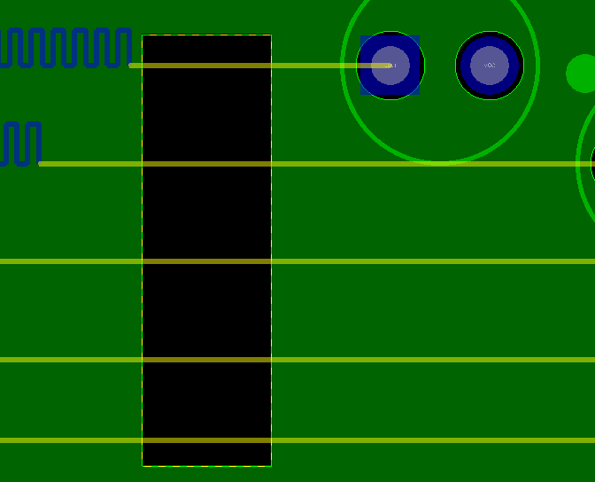
6. Remove the void in the shape using Shape>Manual Isolation/Cavity>Delete then left click the shape (to select it), left click the void boundary then left click again to confirm the deletion. Right click>Done to end the command. You may notice that the segments remain highlighted. You can either use the Route>Slide command to “touch” the cline which will remove the highlight or re-run the command (Display>Segments over voids>Highlight).
Continue through the list and try and resolve all the issues. There are some instances where a cline is only partially covered by a plane and may be exposed around a void for a via or pin (zoom in to examine). Use the Route>Slide command to adjust the routing to clear the void.
7. If you want to close the report the highlighting will remain. To clear the highlighting you can use Display>Segment over Voids>Dehighlight.

End of Lab
All content Copyright 2022 Parallel Systems Ltd.