
All content Copyright 2022 Parallel Systems Ltd.
Start PCB Editor from:
Start (Windows Icon) >Cadence PCB 17.4-2019>PCB Editor 17.4
The PCB Editor Canvas opens.
1. Select File>Open from the PCB Editor main menu.
2. If necessary, set the File Type for Board (*.brd)
3. Use the Browse button to navigate to the C:\OrCAD_Training\PCB_Designer_Advanced directory, select the vision.brd file and left-click on Open.
4. Turn off the top layer and zoom into the middle of the connector J1 as shown below.
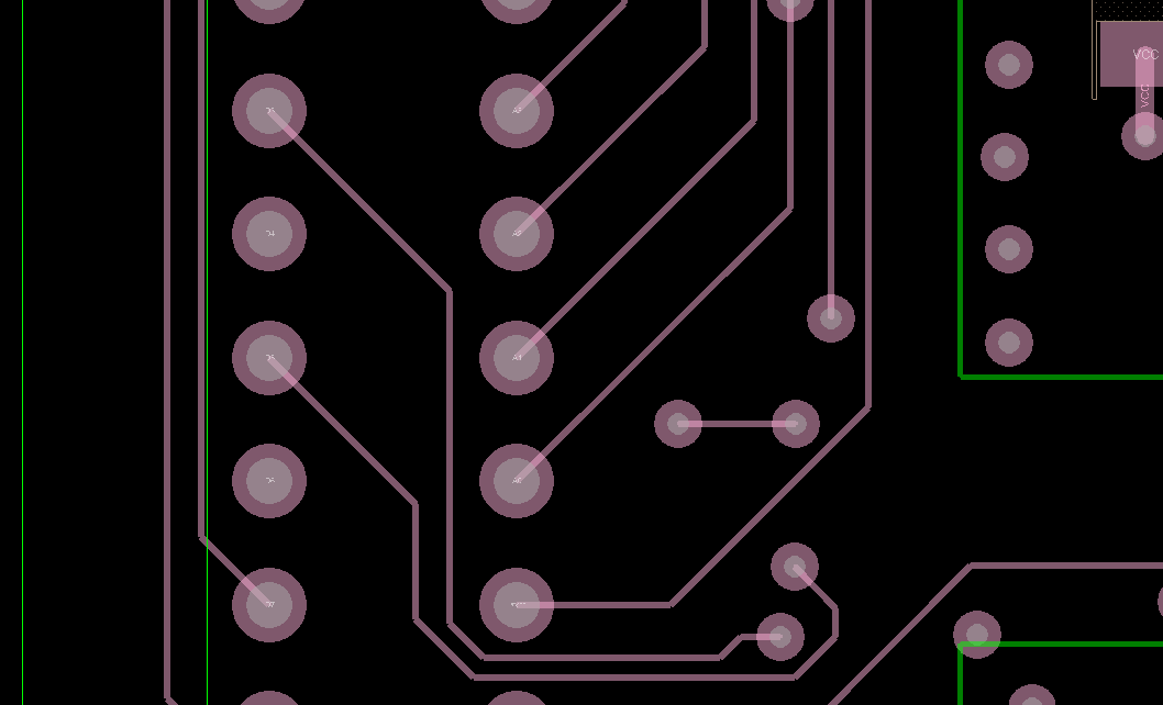
5. Spread between voids only works on the active layer so in the Options pane set the active class to Etch and the subclass to Bottom. Invoke the command Route>Resize/Respace>Spread Between Voids then set the Void Clearance to 1.
6. Left click two pins to set the channel size. For this example pick pins 21 and 53. The two clines between these pins are respaced.
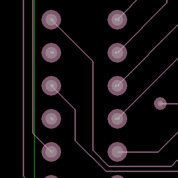
7. Repeat the steps but this time pick pins 14 and 46. The clines are spread out.
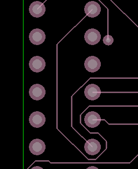
If required, experiment with other clines in the design. Remember to set the active layer as required for this command to work. You do not need to save this design, it will not be used in any further labs.

End of Lab
All content Copyright 2022 Parallel Systems Ltd.