
All content Copyright 2022 Parallel Systems Ltd.
Reference Schematic:
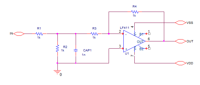
1. Create a new project called Buffer2 and based on Buffer.opj from the previous labs.
2. Delete V1, the pulse stimulus.
3. Remove the circuitry that includes V2 and V3, the supply voltages.
4. Delete the load resistor and capacitor at the output of the LF411.
5. If present, delete the off-page connectors on VDD and VSS.
6. Add hierarchical ports portboth-l left of R1 and on the V+ and V- pins of the LF411.
7. Add an hierarchical port portboth-l to the output node of the LF411.
8. Double-click on each hierarchical port and label, change the Names, as shown in the picture above.
9. Save the design.
10. Select the .dsn file entry form the Project Manager
11. Rename Schematic1 to Buffer_sub
(The name of the subcircuit created will have this name, if you do not change it, the resulting sub-circuit will be called schematic1)
12. Select Tools>Create Netlist from the top menu.
13. Left-click on the PSpice tab.
14. Check the Create Subcircuit Format Netlist check box.
15. Edit the path of the netlist file to your training directory so that you can find it later. (Check that you don’t manage to edit the file name and path to an invalid location)
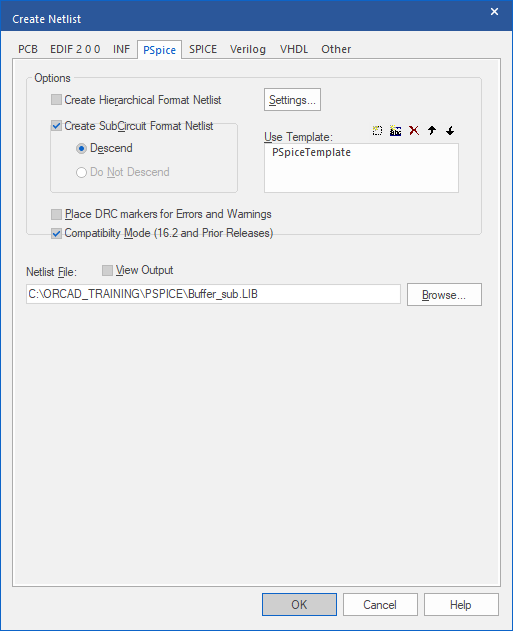
16. Left-click>OK to create the netlist.
17. View the resulting subcircuit by double-clicking on the Outputs folder located within the Capture Project Manager and selecting the library, buffer_sub.lib file.
Note that your listing may vary slightly from the one shown in the following listing by pin order and node names.
Subcircuit Listing:
* source BUFFER2
.SUBCKT Buffer_sub IN OUT VDD VSS
R_R1 IN N00272 1k TC=0,0
R_R2 0 N00272 1k TC=0,0
C_CAP1 0 N00272 1n TC=0,0
R_R3 N00272 N01115 1k TC=0,0
R_R4 N01115 OUT 1k TC=0,0
X_U1 0 N01115 VDD VSS OUT LF411
.ENDS
Note that the “source” of the file in the comment is the design name, rather than the schematic name.

End of Lab
All content Copyright 2022 Parallel Systems Ltd.