
All content Copyright 2022 Parallel Systems Ltd.
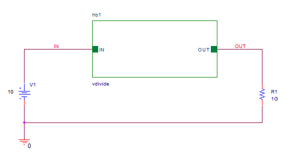
Top level schematic for reference:
1. Start a new PSpice project called Divider based upon the empty project template.
2. Open the schematic page for the project and select Place>Hierarchical Block from the top menu, or left-click on the Place Block toolbar button.
The Place Hierarchical Block dialog box opens.
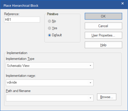
3. Type HB1 in the Reference field.
4. In the Primitive section, check No. (Default will also work)
5. In the Implementation Type pulldown box, select Schematic View.
6. In the Implementation name field type vdivide.
7. Leave the Path and Filename field blank.
8. Left-click>OK.
9. Left-click and drag the mouse to draw the block on the schematic page.
10. If necessary, you can re-size the block by left-click and dragging a corner.
11. If the block is not selected, left-click on it to select it.
12. Choose Place>Hierarchical Pin or left-click the Place H Pin toolbar button.
The Place Hierarchical Pin dialog box opens.
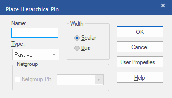
13. Name the pin IN and left-click>OK.
A pin symbol attaches to our cursor.
14. Place the pin on the left side of the block.
15. Place another pin on the right side of the block and name it OUT.
16. Complete the top-level design as shown in the initial figure. Use the VDC and R parts and the 0 symbol.
Note
Remember to change the ground name to 0 if you do not use the 0 (zero) symbol.
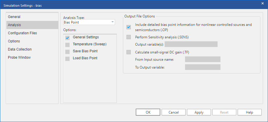
17. Configure a bias point analysis in a new simulation profile.
18. Save the file.
19. Double-click on the hierarchical block just placed, or left-click on it and right-click>Descend Hierarchy, to descend into the page that defines the block contents.
20. Capture will prompt to create a new page, PAGE1, since no underlying definition exists. Two ports will be created to match the Pins added to the block in previous steps.
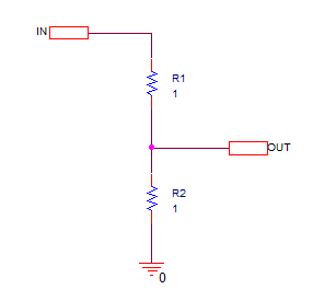
21. Use the two ports provided on the page, two R parts, and the 0 symbol to create the schematic shown below.
22. Save the file.
23. Choose View>Ascend Hierarchy, or press Shift+A to return to the top-level design.
24. Run the simulation.
25. When the Probe window opens choose View>Output File.
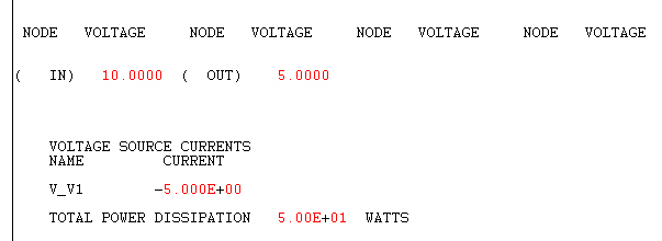
26. Scroll down the output to find the results section. You should see that the voltage on the node OUT is half of the voltage on node IN.

End of Lab
All content Copyright 2022 Parallel Systems Ltd.