
All content Copyright 2022 Parallel Systems Ltd.
1. If necessary, start OrCAD Capture, or Capture CIS, with a PSpice license.
2. Create a new PSpice project called Clipper.
(File>New>Project, Name Clipper, location: C:\OrCAD_Training\PSpice, Enable PSpice Simulation, based on: empty.opj)
3. Open Page1 for the project and draw the circuit as shown below. Use the following parts and symbols:
R, C, VDC, VAC, D1N3940, 0
(Place>Part…, Place>Ground…, Place>Net Alias…)
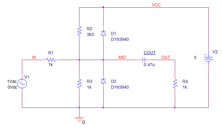
4. Change the reference designator as shown for COUT, which will be underlined.
The other reference designators do not need to match the picture.
5. Edit the value of the VDC source.
(PSpice recognises that a VDC source will have a Voltage value, so 5, 5V or 5Vdc will specify a five volt source)
6. Note the values of the capacitors and resistors and edit the values as needed.
7. Label the nets as shown.
(Strictly speaking the VCC net alias is not required if connected like the example)
8. Create a New Simulation Profile named Clipper_AC.
(Check for the icon in the Task Bar)
9. Left-click Analysis on the left hand side.
10. Select AC Sweep/Noise from the Analysis Type drop-down.
11. Set up the simulation parameters as below:
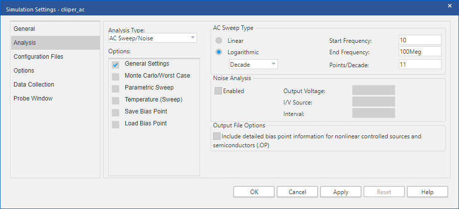
(Logarithmic: Decade; Start: 10; End: 100Meg; Points / Decade: 11)
12. Left-click>OK to save the simulation settings and return to the schematic view.
13. Place markers on the MID and OUT nodes by using PSpice>Markers>Advanced>dB Magnitude of Voltage.
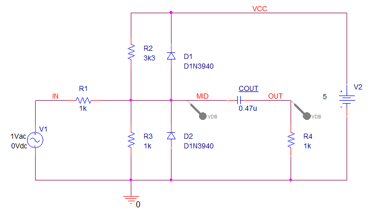
Since the simulation has not been run at this point, and the Probe Window is not open, the Vdb markers will be “grey” until there are results to display.
14. Choose PSpice>Run, or left-click the Run button.
After the simulation has successfully completed, results automatically display within the Probe window.
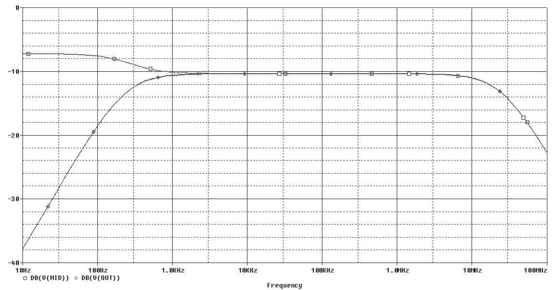
The Probe window displays the dB magnitude (20log10) of the voltage at the marked nets, Out and Mid, as shown. DB(V(MID)) has a lowpass response due to the diode capacitance to ground. The output capacitance and the load resistor act as a highpass filter, so the overall response illustrated by DB(V(OUT)), is a bandpass response. Because the AC Sweep is a linear analysis and the input voltage was set to 1V, the output voltage equals the gain (or the attenuation) of the circuit.
15. Left-click on the name for the trace DB(V(Mid)) located below the X axis of the Probe window.
16. Press Delete to remove the DB(V(Mid)) trace.
17. Choose the Plot>Add Y Axis menu.
18. Choose the Trace>Add Trace menu or use the Add Trace icon, or the Insert key.
The Add Traces dialog box opens.
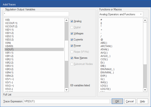
19. Select V(Out) from the list of simulation output variables. Use the vertical scroll bar if necessary
20. Left-click in the Trace Expression field to place the cursor in it.
21. Edit the trace name to be VP(Out) and press the Enter key.
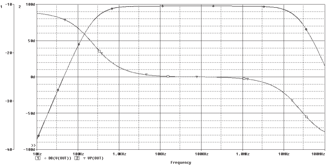
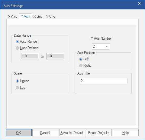
Use the following steps to move the Phase Y Axis to the right hand side of the plot:
22. Select Plot>Axis Settings.
23. Select the Y Axis tab.
24. In the Y Axis pulldown box, select axis 2 and then left-click on the Right radio button to move axis 2 to the right edge of the plot.
Note
Traces can also be built from the “Functions or Macros” on the right hand side of the Add Traces dialog. When a Function or Macro is selected, the expression will be placed in the Trace Expression edit box with the cursor positioned to take the value, or first value, for the expression, selecting a “Simulation Output Variable” from the left hand section will place the selected output variable at the cursor position in the Trace Expression edit box.
As an alternative method, PSpice has a Bode Plot template. Close the Probe window and return to the schematic, select and delete the Vdb probes, from the top menu, select PSpice>Markers>Plot Window Templates, from the Plot Window Templates list, select the “Bode Plot dB – dual Y axes”, left-click>Place, and place the probe on the OUT net. Run the Simulation again and see the resulting Probe display.

End of Lab
All content Copyright 2022 Parallel Systems Ltd.