
All content Copyright 2022 Parallel Systems Ltd.
1. If necessary, open the RC design from Lab 1-1 / 1-2.
2. Select PSpice>New Simulation Profile from the top menu, or left-click the New Simulation Profile icon.
3. Enter RC_bias for the name of the profile.
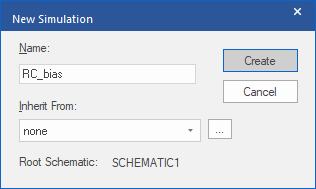
4. Left-click>Create
5. If necessary, left-click Analysis on the left-hand side.
6. Choose the Bias Point option from the Analysis Type drop-list menu.
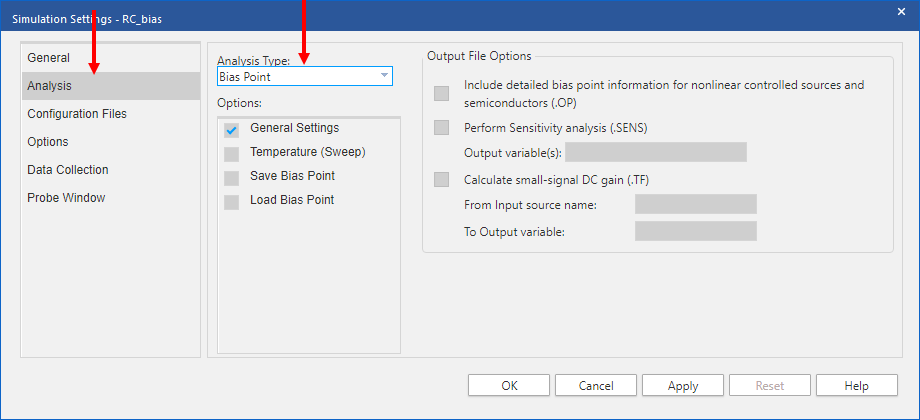
7. Left-click>OK.
The Simulation Setting dialog box closes and the display returns to the schematic page.
8. Select PSpice>Run from the top menu, or left-click the Run  icon.
icon.
The netlister and DRC run automatically and the Probe window opens as shown in the following graphic:
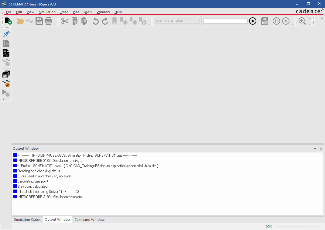
(You may have to left-click on the Probe Window Icon  in the Windows Task Bar to bring the Probe Window to the front)
The Bias Point analysis has a single result so PSpice does not generate any “Probe”, the graphical waveform display, data for bias analysis. Consequently, the Probe window display shown will be empty.
The results of the Bias Point simulation can be viewed from either the output file generated during simulation or from the bias display available from the schematic page.
9. To view results from the output file:
Either:
a) From the active schematic page, choose the PSpice>View Output File menu to examine simulation results in the output file.
Or:
b) From the Probe window, choose the View>Output File menu.
In either case, the results should look similar to the graphic that follows.
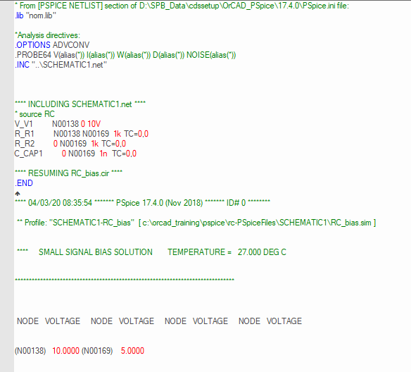
10. Close the output file view, use File>Close to close the view in the Probe Window, or close the tab in Capture.
(Keep the Probe Window itself open in both cases)
11. Select PSpice>Bias Points>Enable from the top menu to turn on the bias displays.
12. Toggle on and off the bias display icons to alter and control the view bias values:
 Voltage markers only
  All Bias markers
(Display of the markers can be controlled from a double-click on an individual marker, or from Net or Part or Pin object Properties)
Optional steps:
Edit the schematic and delete the “0” (ground) symbol and the Run the Simulation again.
What errors do you get? Why?
The error generated is an error that PSpice users can encounter. All SPICE-based simulators require that every analog node has a DC path to ground.
This error is generally caused by either a missing ground symbol or an isolated node between two capacitors.
Replace the “0” (ground) symbol after completing this exercise.

End of Lab
All content Copyright 2022 Parallel Systems Ltd.