
All content Copyright 2022 Parallel Systems Ltd.
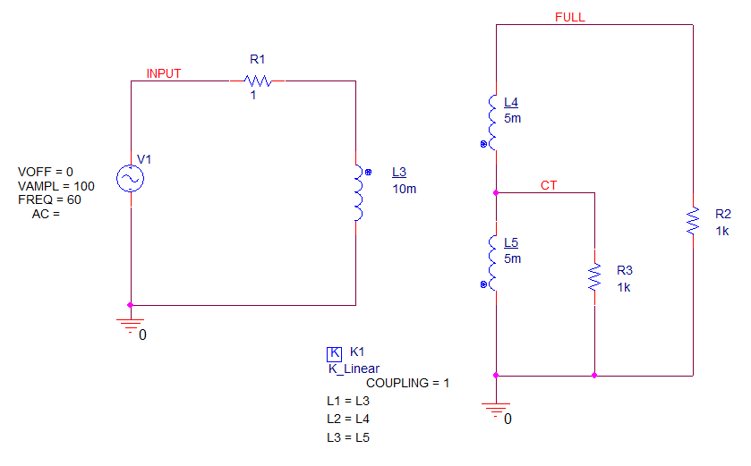
1. Start a New Project named Transformer based upon the empty project template.
2. Open the Schematic and Page and Place parts using the K_Linear, R, L, 0 and VSIN symbols to resemble the circuit above. Note the inductor orientations.
(Leave the K_Linear as the default from the library for now)
3. Wire the circuit together as shown in the above figure.
4. Set the VSIN properties to Offset of 0, Vampl = 100 and Freq = 60
Leave the AC property as the default or, if you do edit the value, set the value to 1 rather than the default “<AC>”
5. Place the Net Aliases for Input, Full and CT
6. Double-click on the K_Linear symbol to edit the properties.
7. Left-click on the Pivot button when the Property Editor tab opens.
Note
Specify the inductors to be coupled by entering their reference designators into the L1 – L6 fields. L1 – L6 will contain the reference designators of the inductors to be coupled, not the values of the inductors.
The inductor values will still be specified on each individual inductor, as normal.
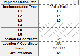
7. Type L3 in the L1 property, L4 in the L2 property, and L5 in the L3 property.
8. If desired, make the L1-L3 properties visible.
This can either be done through the Property Editor or Display Properties.
9. Close the Property Editor and return to the schematic view.
10. Configure a transient analysis with a Run to time of 50mS and a Maximum step size of 0.1m (or 100u)
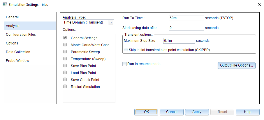
11. Left-click>OK to close the Simulation Settings
12. Add Voltage Probes to the INPUT, CT and FULL nodes
13. Run the simulation and examine the results in the Probe window. The following figure shows the expected results.
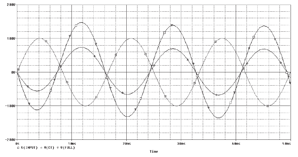
14. Examine the output and note that the centre tapped (CT) node is exactly half of that on the FULL node.
Also make a note of the amplitude of the secondary voltages.

End of Lab
All content Copyright 2022 Parallel Systems Ltd.