


Cadence PCB Mini Option
Available to rent for periods of 1 month
Cadence PCB Mini Option
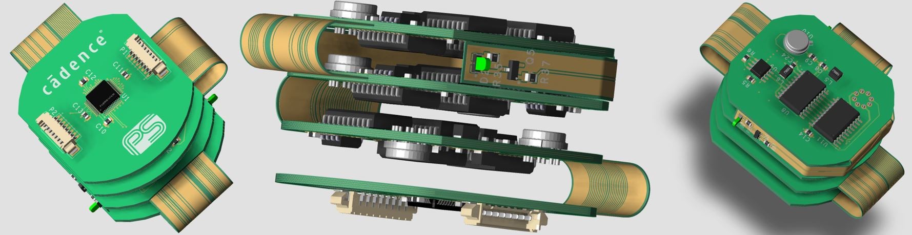
Designers of high-end consumer electronics face the challenge of miniaturization and its resulting complexity. The number of nets on a printed circuit board (PCB) that have high-speed constraints is growing. As the industry migrates to multi-gigabit serial interfaces like PCI Express, the number of constraints on nets is also increasing. And as consumers demand ever-smaller gadgets packed with amazing features, complex die stacking is paramount to an IC packaging strategy.
Today’s PCB and package designers need a complete high-density interconnect (HDI) solution that includes high-speed rules, manages faster data throughput, and offers advanced routing capabilities to shrink footprints and meet aggressive market windows.
PCB Mini Option Tutorial Videos
| VIDEO | Constraint Manager: HDI rule set |
| VIDEO | Micro-via and associated spacing, stacking and via-in-pad rules |
| VIDEO | Constraint driven HDI design flow |
| VIDEO | HDI micro-via stack editing |
| VIDEO | Manufacturing rule support for embedding components |
| VIDEO | Embed components on inner layers |
| VIDEO | Support for Cavities on inner layers |
| VIDEO | Support for Vertically placed components on inner layers |
| VIDEO | Dual Side Contact Embedded Components |