
Precision EDA since 1997
Electronic design automation, engineered with purpose.
Welcome to Parallel Systems, your partner for Cadence PCB design EDA software, training and engineering services. We supply OrCAD X, Allegro X, Sigrity X and AWR RF design software, as well as Allegro X AI tokens and SiliconExpert component intelligence. We support electronics companies across the UK, Ireland, Gibraltar, Guernsey and Jersey with EDA Software, design translation, ECAD library development and maintenance, RF antenna consultancy, including beam-steering and MIMO systems. With expert guidance, competitive pricing and dedicated support, we help you choose the tools and services that fit your business.
Explore the site
Everything we offer, one click away.
Design software, AI, simulation, RF, data management, resources and support
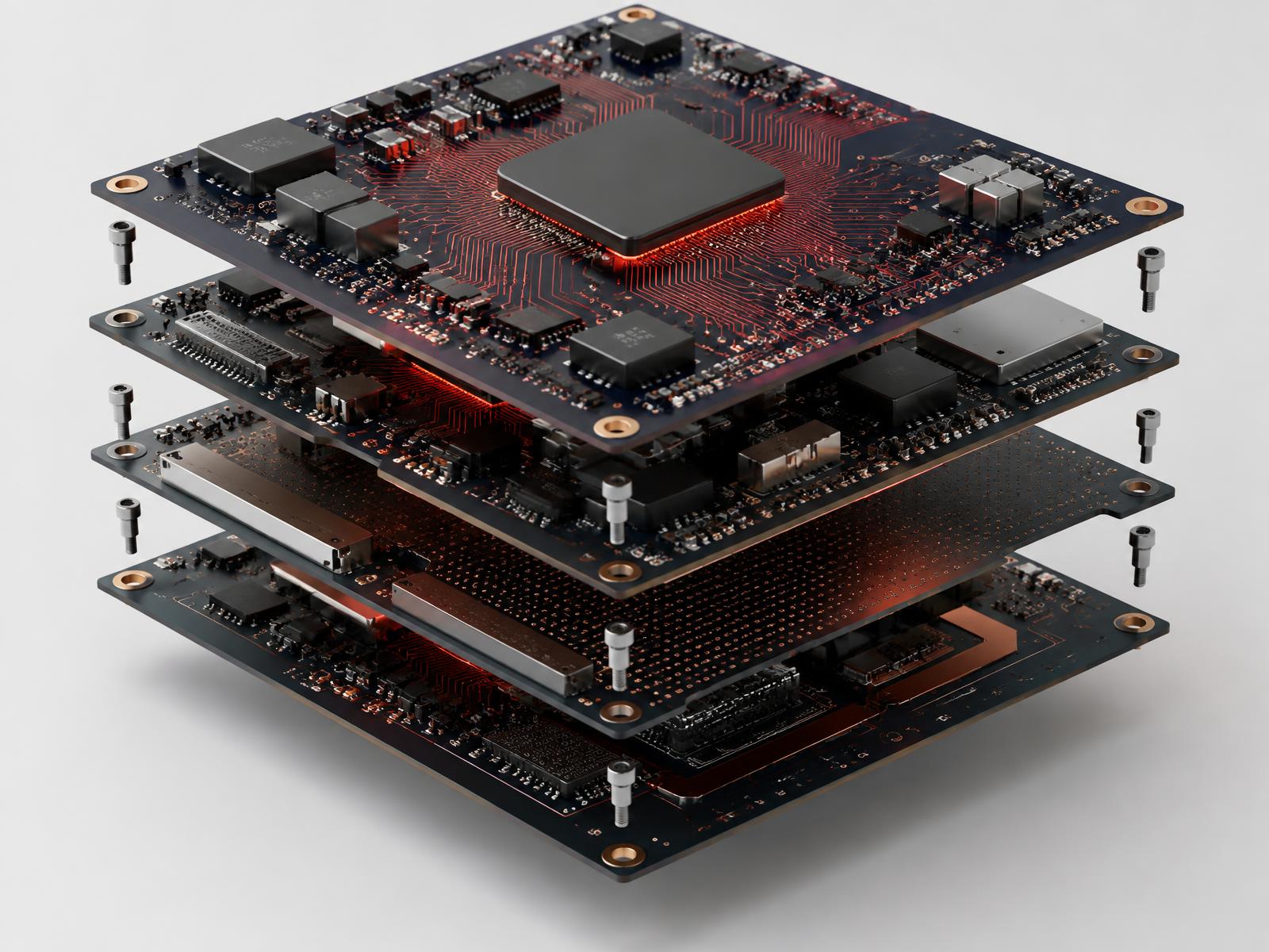
01 / PCB design
Allegro X
Constraint-driven schematic capture and PCB layout for complex, high-density and multi-board designs.
Explore Allegro X
02 / Generative AI
Allegro X AI
AI-assisted placement, routing and power plane creation that turns hours of layout into minutes.
Discover Allegro X AI
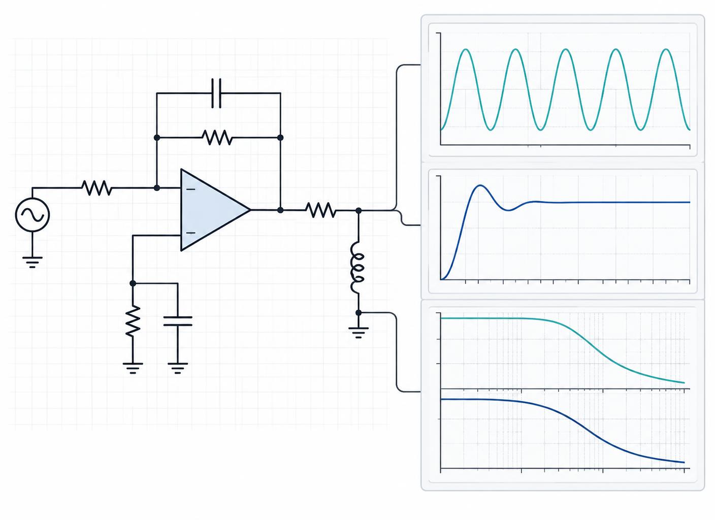
03 / Simulation
PSpice
Analog and mixed-signal circuit simulation to prove your design before the first board is built.
Explore PSpice

04 / Integrity
Sigrity X
Signal and power integrity analysis that finds high-speed problems early in the design flow.
Explore Sigrity X
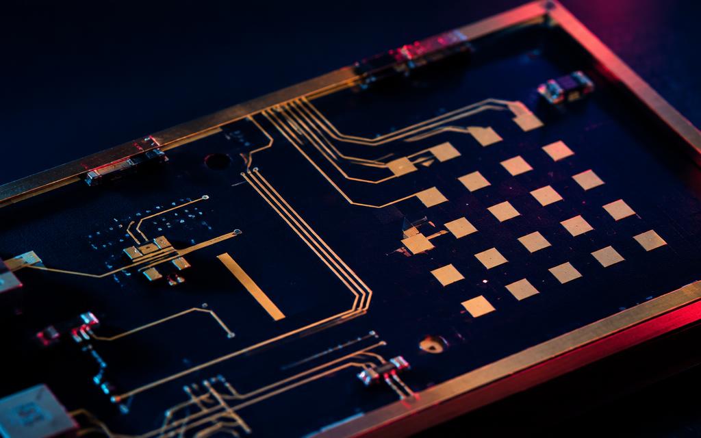
05 / RF & microwave
AWR
Microwave Office and Visual System Simulator for RF, microwave, antenna and MMIC design.
Explore AWR
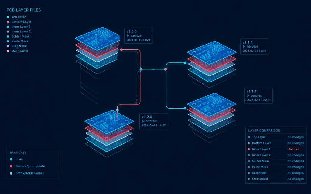
06 / Data management
EDM
Keep libraries, designs and revisions under control so your whole team works from one source.
Explore EDM

07 / Components
CIP
Component information and library management linked to live part data for OrCAD and Allegro.
Explore CIP
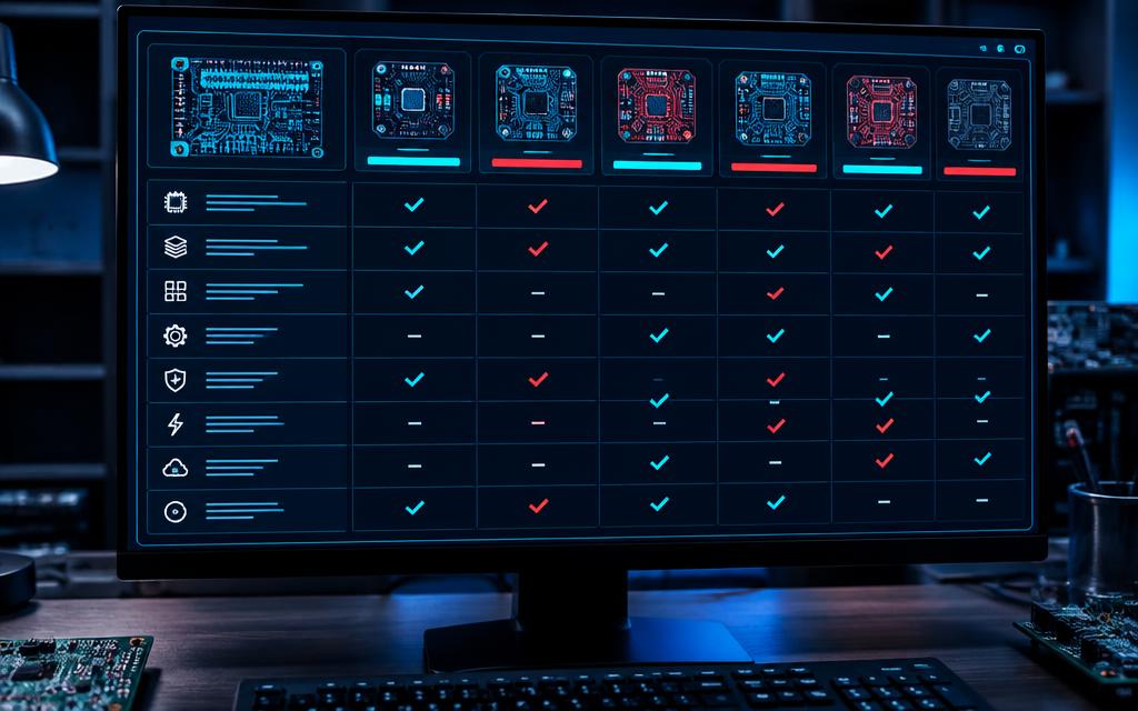
08 / Compare
Feature matrix
Compare OrCAD X and Allegro X editions side by side, with video walkthroughs for features.
Open the matrix
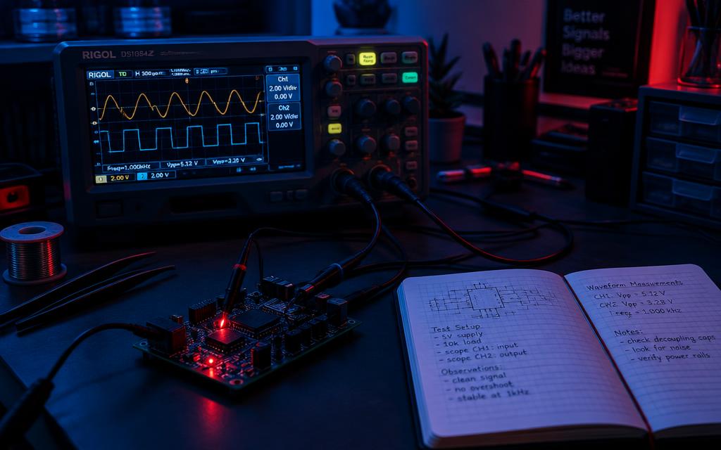
09 / Resources
Guides
Practical how-to guides and videos to help your team get more from Cadence tools.
Browse guides

10 / Services
Design bureaus
Find trusted PCB design bureaus across the UK and Ireland using Cadence tools.
Find a bureau

11 / Customers
Testimonials
Hear from engineering teams who rely on Parallel Systems for software, training and support.
Read testimonials

12 / Talk to us
Contact
Ask about pricing, licences, training or evaluations — our UK team is ready to help.
Get in touch
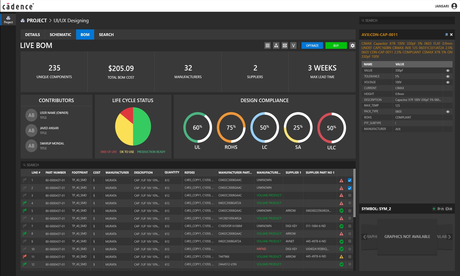
13 / Collaboration
Allegro Pulse
Connect design teams, libraries and supply chain with automatic version control, LiveBOM and enterprise collaboration.
Explore Allegro Pulse
Customer stories
Designed with Cadence Allegro X
VSORA
Designed with Cadence Allegro X
SpiNNaker
Designed with Cadence Allegro X
Raspberry Pi
Designed with Cadence Allegro X