The fully integrated engineering experience you've been waiting for.
Overview
Modern schematic authoring for multi-board systems
This modern schematic authoring solution is built from the ground up with multi-board systems and concurrent engineering in mind. Collaboration is seamless and secure with multi-user team design, powerful version management, and flexible access control. The tight integrations into AWR Design Environment Platform, Sigrity X Platform, electromagnetic (EM) analysis, thermal analysis, and PSpice technologies makes Allegro X System Capture the fully integrated engineering experience you've been waiting for. With fast wiring and interconnectivity, teams can manage large pin counts and complex signal handling effortlessly with net and port groups, electrical constraint sets, and smart wiring features for accurate and efficient design.
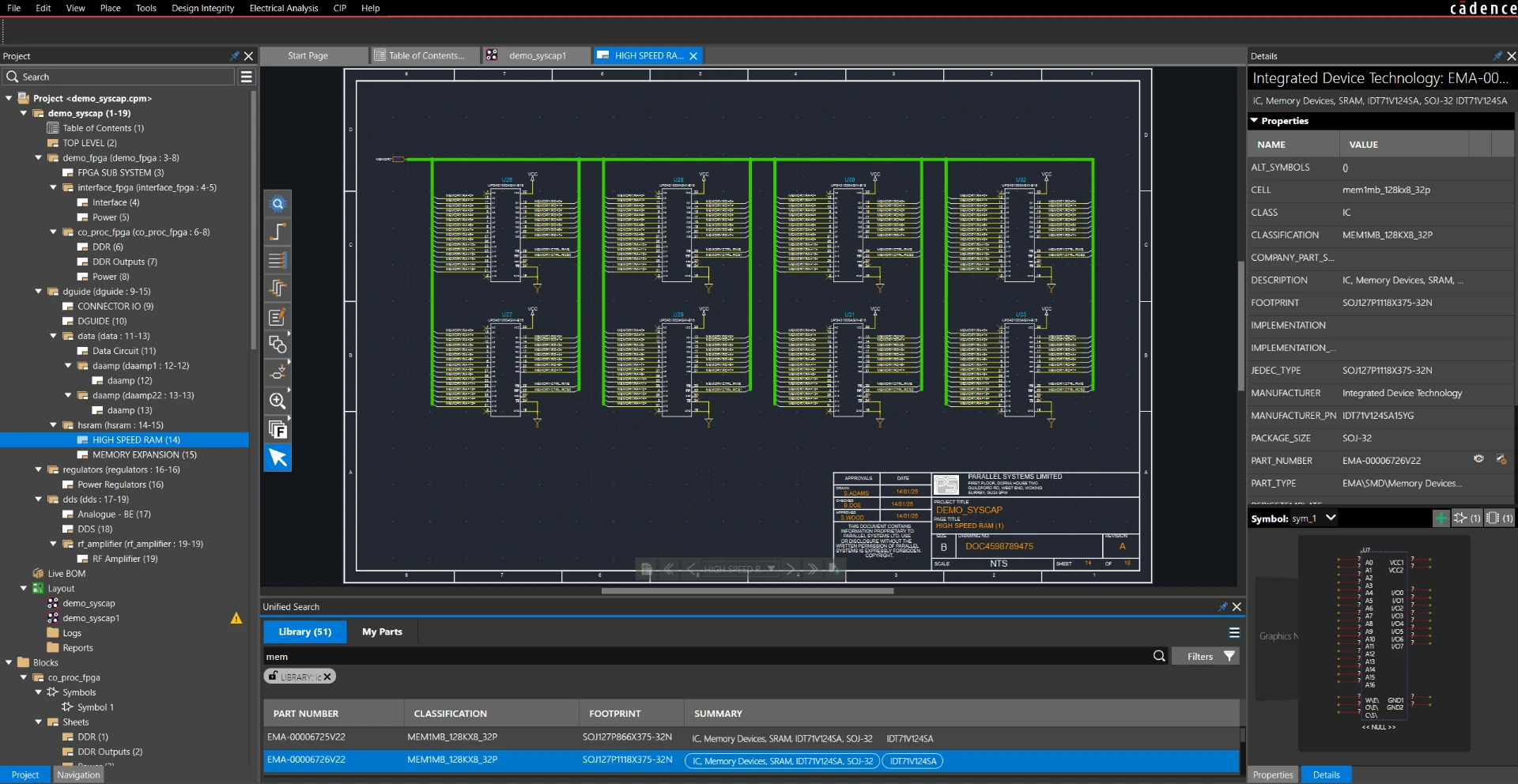
Integrated library and unified part search allows teams to update part and model information with ease, as well as search in your curated library network for the exact reference information necessary for your designs.
Built with reuse and version control in mind, Allegro X System Capture enables your engineers to customize and templatize repeatable sections to ensure that they don't have to lay out the same pin array on several unique occasions, while allowing multi-user access and editing capabilities at both block and page levels for secure and collaborative design management.
Validate your electrical designs and prevent common errors with access to advanced electrical rule checks and intelligent defaults. Easily configure your design checks, parameters, and power and ground rules to meet your specific design requirements with dynamic notifications of any violations.
With an always up-to-date bill of materials (BOM), complete with real-time supply chain insights, electrical engineers can make data-driven decisions and keep track of the parts needed to mitigate any design risk and ensure the timely delivery of products.
Design for reliability
MTBF and stress analysis built in
Leverage model-based design, electrical overstress (EOS), and mean time between failure (MTBF) analysis to ensure all components function as intended.
Capabilities
Advanced Tools for Seamless PCB Design and Management
Allegro X Design Platform helps bring your innovative and bleeding-edge designs to life. The constraint-driven environment provides instantaneous visual feedback and ensures the functionality and manufacturability of your PCBs while allowing you to keep designing.
Library and Design Management
Create, share, and manage your libraries and design data from a centralized environment. Team members have access to up-to-date information, enhancing collaboration and reducing errors. Robust version control features help keep track of any changes and maintain a complete history of revisions, ensuring data integrity.
Design for Reliability
Leverage model-based design, electrical overstress (EOS), and mean time between failure (MTBF) analysis to ensure all components function as intended for reliable, long-lasting product that meet regulatory standards.
Design Reuse
Not every project you work on must start from scratch. With existing and proven design IP, you can save time and prevent design errors. By reusing known-good schematic blocks, PCB modules, and design constraints, you can easily streamline your engineering process and get to market with verified technology faster.
SPICE Simulation
PSpice technology offers accurate and advanced circuit analysis for your PCB designs and ensures compliance with ISO 26262 standards for functional safety in automotive systems. With true analog and mixed-signal simulation, easily simulate and verify the behavior of your circuits before physical prototyping. Tailored for precision electronics, consumer, high-power industrial equipment, and high-reliability applications.
Constraint-Driven Design
With a real-time constraint-driven flow, you can easily set up your physical, electrical, spacing, 3D, and manufacturing design rules to visually verify that your unique requirements are being met. This way you'll have less stress at signoff, reduce design respins, and improve time to market.
Rigid-Flex
Stack-up by zone allows you to create and manage advanced, multi-layered stackups for both rigid and flexible regions of your PCB. Easily define bend areas and specify material requirements, while utilizing the 3D visualization tools to ensure proper form and fit. Utilize inter-layer checks to ensure the integrity and reliability of your designs to prevent potential issues during manufacturing.
In-Design Analysis
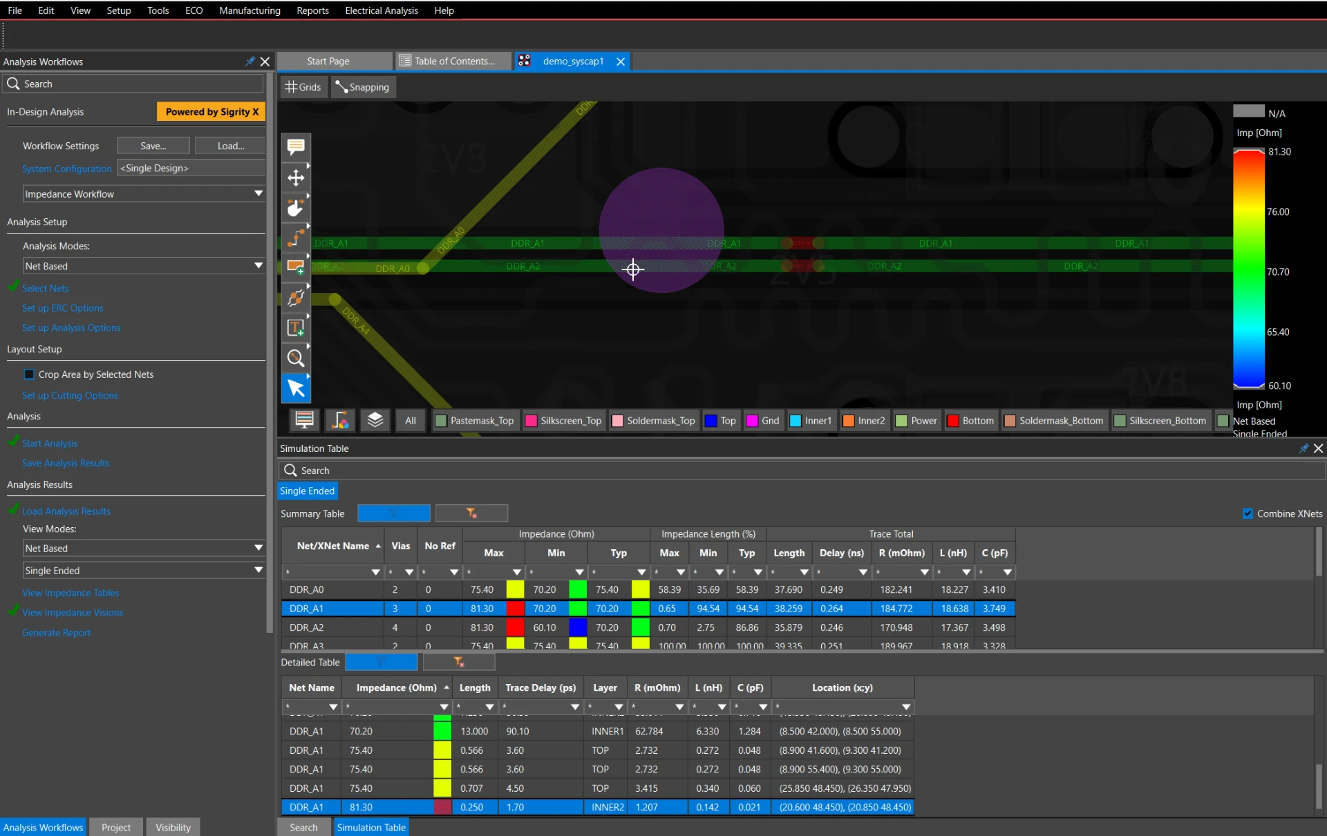
Leverage Cadence's award-winning simulation technologies and solvers to analyze and evaluate your circuits and designs without ever leaving your schematic or PCB canvas. Sigrity, Clarity, and Celsius solvers provide workflows for checking impedance, crosstalk, return path, IR drop, temperature rise, reflection, and more, all with minimal setup thanks to intelligent defaults and on-the-fly model creation.
ECAD-MCAD Co-Design
Simplify the sharing of design data. Strong integrations to MCAD tools such as Autodesk Fusion, Dassault Systèmes SOLIDWORKS and CATIA, Siemens NX, and PTC Creo allows for bi-directional exchange of mechanical and electrical data.
Concurrent PCB Team Design
Collaborate seamlessly with global PCB design teams through a shared canvas, ensuring consistency and eliminating the need for copy/paste. Maintain consistency across projects as updates occur in real time, allowing for split-second design decisions while streamlining the design cycle.
Design for Manufacturing
Real-time design for manufacturing (DFM) checks, including design for fabrication (DFF), design for assembly (DFA), and design for test (DFT), can help you identify potential problems while you design, so that you can avoid costly respins which ultimately derail your project timeline.
PLM Integration
Access out-of-the-box connectors for all the major PLM systems from Oracle/Agile, PTC Windchill, Siemens Teamcenter, Dassault Systèmes 3DEXPERIENCE and 3DEXPERIENCE WORKS. Once connected to PLM, you will have up-to-date part information supplied by the PLM system and the ability to update the PLM with the current BOM, 3D model data, and manufacturing deliverables with a single click.
Generative PCB Layout
Combining traditional physical design algorithms with generative AI techniques, Allegro X AI produces compelling placement of components on the PCB. Exploring a much larger solution space than what is possible through manual methods, the technology drives optimization of metrics, such as shorter wire lengths, while adhering to the design constraints.
Packing complex technologies in a small area has its challenges, but with HDI technology and embedded components, it's possible to maintain signal integrity and performance. Shorter signal paths and via stub elimination make it easy to create reliable, powerful, and compact designs.
In-design analysis
Reliability engineering
Understanding MTBF in schematic design
MTBF (Mean Time Between Failures) is a statistical reliability metric: the average operating time a system runs between consecutive failures. In electronics it is calculated as total operating time divided by the number of failures over that period and, under the constant-failure-rate assumption used for most electronic components, it is simply the inverse of the failure rate.
Strictly, MTBF applies to repairable equipment; for a non-repairable part (a resistor, an IC, a disposable module) the technically correct term is MTTF (Mean Time To Failure), though the industry routinely uses MTBF for both.
How it relates to schematics and circuit design
In a schematic or BOM context, MTBF usually means a reliability prediction done against standards such as MIL-HDBK-217F or FIDES.
Step 1
Every part is assigned a base failure rate, adjusted for temperature, electrical stress (voltage derating), quality level and environment — e.g. λp = λb × πQ × πT × πV × πE in MIL-HDBK-217F.
Step 2
All component failure rates are summed to give a system failure rate, then inverted: MTBF = 1 / λsystem.
This is why schematic-level choices directly move the number: derating a capacitor, choosing a higher-grade part or reducing junction temperatures improves the predicted MTBF. It also explains why one weak component drags down the whole figure — a system's reliability can be no better than its least reliable component.
Why it matters
Design comparison and qualification
Compare designs, alternative parts and vendors before building hardware, and check whether reliability goals are achievable. Often contractual in military, telecom, medical and industrial markets.
Warranty, spares and maintenance
A higher MTBF means fewer expected field failures, which drives warranty cost, spare-parts stocking and service scheduling.
Sales and customer conversations
Datasheet MTBF figures (common on power supplies and DC-DC modules) are a standard way buyers compare reliability between suppliers.
Common misconceptions
MTBF is not life expectancy. A 1,000,000-hour MTBF does not mean a unit lasts a million hours; it is a statistical average. Only about 37% of units survive to their MTBF figure, and a 100,000-hour MTBF roughly means half the products could fail by 50,000 hours.
It covers random failures only. Parts-count predictions exclude wear-out mechanisms such as solder-joint fatigue, electrolytic capacitor drying or connector wear, which often dominate real product life.
Standards differ and can be pessimistic. MIL-HDBK-217F has not been updated since 1995 and tends to overstate failure rates for modern commercial parts, while Telcordia SR-332 is generally more realistic for commercial and telecom hardware.
In short: in schematic work, MTBF is the quantitative output of a reliability prediction driven by your parts list and how hard you stress them — useful for comparing designs and setting warranty and service expectations, but not a guarantee of how long any individual board will last.
MTBF in Allegro X System Capture
MTBF estimation directly from the schematic with no simulation models required — accuracy improves when detailed electrical overstress (EOS) results refine the failure rates.
Reliability standards support: adheres to the FIDES standard, with MIL-HDBK-217F support for real-time reliability analysis.
One integrated reliability flow: schematic audit (30+ integrity checks, no models needed), overstress/derating analysis and MTBF reports, with cross-probing back to the schematic.
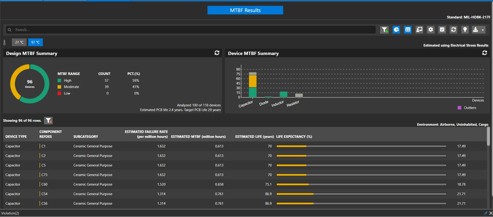
A results dashboard shows the design summary and estimated PCB life expectancy, highlighting the components dominating the failure rate.
Bring schematic capture, simulation and team design into one connected flow.
Allegro X System Capture keeps your libraries, constraints and analysis in step from first schematic to final layout.