
Allegro X Design Platform
Redefining system design with greater productivity
Cadence Allegro X. An integrated environment for PCB and multi-board electronic system design. Concurrent collaboration, constraint-driven workflows and integrated analysis help teams reduce project risk and shorten design cycles.
Platform overview
One connected engineering workflow
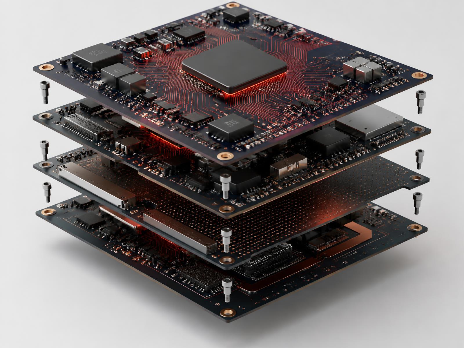
Allegro X brings schematic capture, PCB layout, design data management and in-design analysis together in a single connected workflow — so engineers work from the same data, at the same time.
- Schematic capture
- PCB layout
- Design data management
- In-design analysis
Built for collaboration and scalable system design, the platform supports data-informed engineering decisions from first schematic to manufacturing.
Key benefits
Built for how system teams actually work
Engineering cockpit
Unified schematic, PCB layout and in-design analysis, with centrally managed, versioned design data.
Multi-domain system design
Coordinated electrical, mechanical and thermal workflows across the whole system.
Augmented intelligence
Tools that help engineers explore design options and improve performance and cost.
Verification and optimisation
Integrated simulation and analysis workflows, including Optimality Intelligent System Explorer.
Data integrity and security
Access control, encryption, versioning and managed collaboration.
Multi-discipline team design
Concurrent schematic and PCB design using shared project data.

Applications & team workflows
Every discipline, one design
See how each role contributes to the same shared project.
PCB designers
Place, route and verify boards against live constraints, sharing the same database as the rest of the team. AI-assisted placement and routing take repetitive tasks off the critical path.
↳ One shared, versioned design database
Why Allegro X
The enterprise PCB design platform
Cadence Allegro X is the strongest enterprise-grade PCB design platform available because it combines schematic capture, advanced PCB layout, constraint management, SI/PI/thermal analysis, MCAD collaboration, library governance, and AI-assisted design in one connected environment. Rather than treating PCB design as isolated CAD work, it connects electrical, mechanical, manufacturing, and supply-chain decisions throughout the product lifecycle.
Why it stands out
Allegro X is especially compelling for complex, high-speed, high-reliability, multi-designer, or enterprise products, such as networking, automotive, aerospace, RF, power electronics, and advanced digital systems.
| Capability | Why it matters |
|---|---|
| Unified schematic, layout, and analysis | Engineers can move between logical and physical design without losing context, reducing iteration cycles. |
| Constraint-driven high-speed design | It manages timing, impedance, differential pairs, crosstalk, reflection, SSN, creepage/clearance, and DFM rules, supporting a “correct-by-construction” workflow. |
| SI, PI, thermal, and EM analysis | Issues such as IR drop, impedance discontinuities, return paths, power delivery, and thermal problems can be found earlier. |
| Concurrent multi-user collaboration | Several designers can work in the same design database simultaneously, with changes updated in real time. |
| AI-assisted placement and routing | Allegro X AI can automate placement, copper pours, and critical-net routing, with Cadence claiming turnaround reductions of 10x or more for relevant tasks. |
| MCAD and enterprise integration | Bidirectional links with major MCAD tools keep PCB and mechanical data synchronized and version-controlled. |
| Library and sourcing intelligence | Ultra Librarian integration provides searchable IPC-compliant symbols, footprints, 3D STEP models, and real-time distributor stock, pricing, and authorized-supplier data. |
Benefits by user level
| Role | Key benefits |
|---|---|
| Junior PCB designer |
|
| Experienced PCB designer |
|
| Electrical / hardware engineer |
|
| SI/PI or RF engineer |
|
| CAD librarian |
|
| Engineering manager |
|
| Programme / product manager |
|
| Manufacturing, NPI, and quality teams |
|
The business case
Allegro X’s main value is not simply that it is a powerful PCB editor. It's that it turns PCB design into a governed, collaborative, analysis driven, product development process. Cadence positions the platform around concurrent engineering, integrated signoff-level analysis, real-time collaboration, and AI-enabled automation; claiming productivity improvements of up to 4x for complex system design and more than 10x turnaround reduction for AI-assisted placement and routing tasks.
Allegro X is the best premium, enterprise PCB system for teams whose boards are complex, high-speed, reliability-critical, or produced by multiple engineering disciplines.
For an organisation designing sophisticated electronics, that translates into:
- Faster time to market.
- Fewer re-spins and lower prototyping cost.
- Higher first-pass success.
- Better high-speed and power-integrity outcomes.
- Cleaner component libraries and fewer sourcing risks.
- Improved collaboration between electrical, mechanical, manufacturing, and supply-chain teams.
Testimonials
What engineering leaders say
“At Schneider Electric, turnaround time and the quality of the end product are absolutely critical for business success. With the Allegro X AI technology from Cadence, we see a great potential to significantly shorten our development cycle.”
Customer success
Designed with Cadence Allegro X
VSORA
Designed with Cadence Allegro X
SpiNNaker
Designed with Cadence Allegro X
Raspberry Pi
Designed with Cadence Allegro X
Capabilities
From library to manufacturing
Component libraries and simulation
Integration with Ultra Librarian, access to over 18 million IPC-7351B and ANSI-compliant symbols, footprints and 3D STEP models, plus PSpice models.
Constraint-driven design
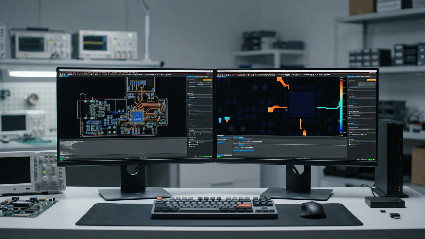
Electrical, physical, spacing, manufacturing and other rules with visual feedback.
Concurrent engineering
Multiple designers working on shared design data with real-time updates.
System analysis
Signal integrity, power integrity, thermal and electromagnetic analysis — including impedance, return path, IR drop and temperature.
Design management and AI-powered automation
Library and version management, AI-assisted placement and routing, and advanced-substrate design rules.
ECAD-MCAD co-design
Bi-directional exchange with Autodesk Fusion, SOLIDWORKS, CATIA, Siemens NX and PTC Creo.
Reliability
PSpice simulation and checks such as MTBF and electrical overstress.
Design for manufacturing
DFM, fabrication, assembly, test, interlayer and HDI checks.
Timing and phase constraints
Visual length and phase constraints using the Allegro X TimingVision environment.
Supply-chain visibility
Sourcing intelligence, availability and pricing, supplier verification and part-alternative evaluation.
Product matrix
Which PCB design suite is right for you?
Compare OrCAD X and Allegro X editions side by side — hundreds of PCB design features, options and linked video demonstrations in one searchable table.
Video overview
The PCB design suites and options explained
A quick tour of the OrCAD X and Allegro X PCB suites and the options available for each.
Products
Part of the Allegro X family
Allegro X PCB Designer
Constraint-driven PCB layout for designs from simple to highly complex, with integrated schematic, rigid-flex, HDI and manufacturing outputs.
PSpice
Industry-standard analogue and mixed-signal circuit simulation for verifying and optimising circuit behaviour before layout.
Allegro X AI
AI technology built on the Allegro X platform that automates placement, power-plane generation and critical net routing.
Features
Feature overview
- Library and design management
- Centralised, versioned libraries and design data.
- Design for reliability
- Stress and reliability checks driven by simulation.
- Design reuse
- Reuse proven circuit and layout blocks across projects.
- SPICE simulation
- PSpice analogue and mixed-signal simulation.
- Constraint-driven design
- Rules defined once and enforced from schematic to layout.
- Rigid-flex design
- Layer-stack and bend-aware rigid-flex layout.
- In-design analysis
- Sigrity, Clarity and Celsius workflows inside the design flow.
- ECAD-MCAD co-design
- Bi-directional exchange with major MCAD tools.
- Concurrent PCB team design
- Several designers working in one database simultaneously.
- Design for manufacturing
- DFM, assembly, test and HDI checks.
- PLM integration
- Connect design data with enterprise PLM systems.
- Generative PCB layout
- AI-driven placement and routing exploration.
- Miniaturisation and HDI design
- Microvias, fine-pitch and dense interconnect support.
Free viewer
Share, Explore, and Review Designs in Detail with the Allegro X Free Viewer
Stakeholders across engineering, manufacturing and management can open, inspect and review Allegro X designs without a full design licence.
Download the Allegro X Free Viewer