2. Entering the Schematic
This section describes how to use OrCAD© Capture-PSpice© to enter the schematic for the Headphone Amplifier example design.
Note: The instructions throughout this worked example assume some familiarity with the concepts of entering a schematic, running a simulation and designing a board, if necessary, please get some familiarity with these basic tasks before attempting to work through this example.
Starting the Project
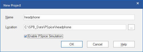
Begin by starting OrCAD Capture, or OrCAD Capture CIS, any licensed version, including the OrCAD Trial, may be used for this example. Then, in the opened Capture application, use File>New Project to start a New Project, name the project Headphone, for example, check the Enable PSpice Simulation, and specify a folder for the project location.
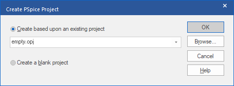
Base the new project on the empty.opj existing project when prompted for a project template.
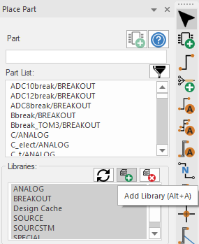
Adding the Libraries
Start by adding the Libraries. Left-click on the "+" for "headphone.dsn" and then the "+" for "SCHEMATIC1", double-click on the Page1 entry to open the Schematic Page. Left-click in the Schematic Page to activate it and the use use Place>Part from the menu. In the Place Part form at the right, left-click the Add Library icon to open a browser for the required libraries.
When the file browser opens to select the libraries, add all of the libraries from the default location: C:\Cadence\SPB_17.4 then tools\Capture\library\PSpice for the PSpice libraries with left-click on the first, 1_shot, library then scroll down to the end of the list of files and shift+left-click select the last, Zetex, library, then left-click>Open to add the selected libraries.
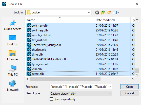
(The default library path for the regular Capture library parts will be: C:\Cadence\SPB_17.4 then tools\Capture\library. If you installed to a location other than the default, you will need to adjust the root directory to reflect your installation settings for both library locations.)
Placing the parts
Use the completed schematic in the Introduction for this example for reference as you enter the schematic. The exact layout of the schematic is not critical to having a working example but correctly connecting the various elements will be required to get the circuit to work as expected. Once the libraries have been added, place the POT from the Breakout library, from the menu, Place>Part, type POT in the "Part" edit box and press enter to get the POT graphical part on the mouse cursor. (If necessary, select the Breakout entry if it is not already selected within all of the libraries, blue background)
Use right-click>Rotate, or press the R key on the keyboard, to rotate the POT so that the "Resistor section" is vertical with the wiper pin to the right, or left, of that, then left-click the mouse to place the POT part towards the upper left of the page, right-click>End Mode, or use the Esc key, to end placing.
Note that which "end" of the POT that the wiper is connected to will not be critical, PSpice will be used to simulate the circuit bias to evaluate the required set point for the POT.
Double click on the POT symbol and change the Value property from the default 1k to be 50k and close the property editor tab, accept any changes; or double-click on the 1k text and change the text value to 50k, then left-click>OK to set the value. In both cases note that the value of the POT should now be 50k, rather than the default 1k. If required, left-click on the SET=0.5 text and drag the mouse to move this text away from the POT pin so that any added wires do not obscure the text.
Use File>Save from the menu to save the current schematic.
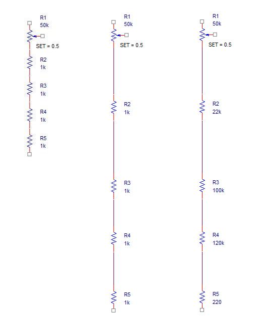
Next place the four resistors to complete the input bias chain, these will be R from the Analog library, again rotate the resistor symbol so that they are vertical, drop the resistor pins together, right-click>End Mode, or use the Esc key, to end the placing command and then drag the resistors to get the wires added.
Use File>Save from the menu to save the current schematic.
Once the wires have been added change the value of the resistors to meet the requirements of the circuit, double-click on the default 1k value and change the text to the required values. Don't be too concerned about the exact placement of the components at this stage, their positions can be changed as the circuit is completed.
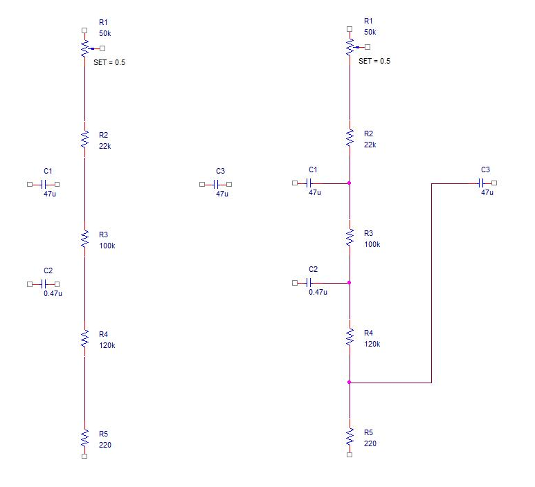
Next place the three capacitors, C1 to C3. Also note that, as far as PSpice is concerned, Capacitors are not polarised, regardless of value, so the C part from the Analog library will be used. Note that actual circuit components probably will be polarised for the larger values. Change the values from the default 1n values to the values required for the circuit. Then use Place>Wire from the menu, or the W key, to enter wiring mode and make the initial connections, as shown, left-click on a pin to start the wire, move the mouse to draw the wire, left-click to add any corners to the wire and left-click on the destination pin to complete the connection(s), right-click>End Mode, or use the Esc key, to end wiring mode. (Note that the right hand half of the image has the wires attached to the capacitors.)
Use File>Save from the menu to save the current schematic.
Now continue to place and wire the next stage of the schematic. When placing the BC212 PNP transistor, use right-click>Mirror Vertically while the part is on the cursor to get the emitter at the top of the part. The BC182BP and BC212AP parts can be placed from the Zetex library.
(These parts can also be located from Place>PSpice Component>Search. When the PSpice Part Search form opens at the right, enter the part name to search for and left-click the search icon. There is a local database which is searched for the parts in the provided libraries. Double-click on the item in the list to add it to the cursor for placement in the Schematic Page)
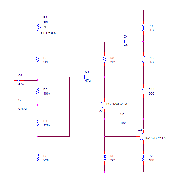
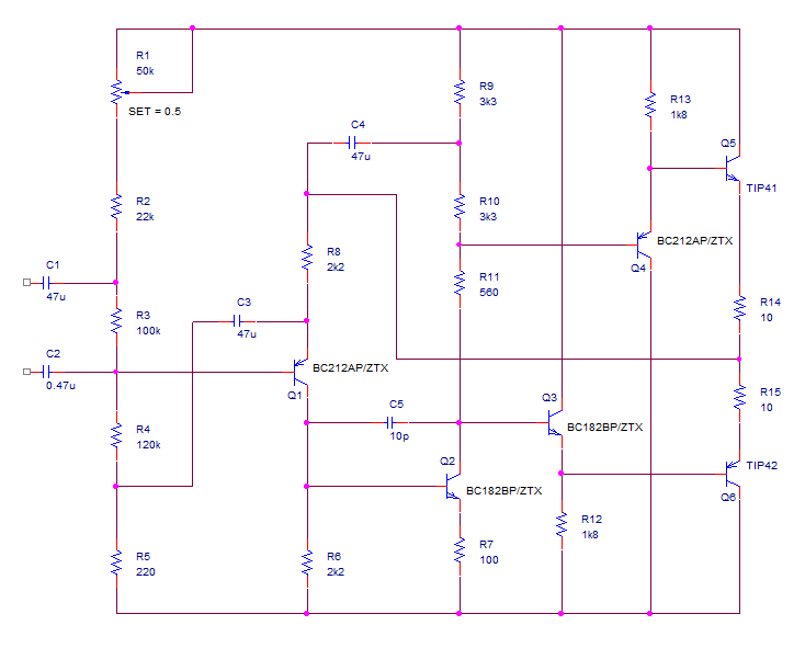
Now continue with the schematic, working towards the right, use the "Mirror Vertically" option when placing the PNP transistors to get the Emitter towards the "top", or "bottom", as required. Also add the connection for the wiper of the POT component and the TIP41 and TIP42 transistors from the Pwrbjt library, with associated resistors from the Analog library.
Use File>Save from the menu to save the current schematic.
So far, all of the wires have default, system assigned, names, these will be formatted as "N" followed by an identifying number. Whilst these names will work perfectly as far as the design is concerned, it will be much easier to identify key net names if the default net names are overridden with Net Aliases. From the menu, Place>Net Alias (or press the N key), this form will open:
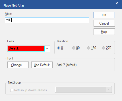
Then type in the required Net Alias name to assign in the Alias field, the value needs to be MID in this case, and left-click>OK. The Net Alias value will be attached to the cursor and can be applied to a net by clicking on the net to "stick" the Net Alias to it.
(Some things to note about placing Net Aliases: IF the Net Alias ends in a number, the number will be automatically incremented, so a value of A0 will become A1 and so on, it is not possible to disable this; The Net Alias value will remain on the cursor so that it can be assigned to other wires, note that nets of the same name on the same schematic page will automatically be connected by the netlister so don't "accidentally" apply the same Net Alias to nets that you do not intend to have connected.)
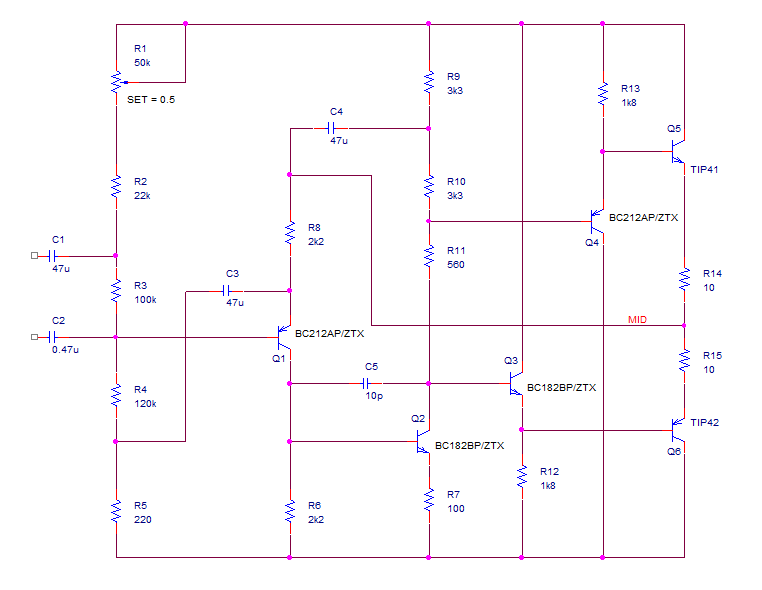
Net Alias "MID" shown assigned to the wire at the junction of the two output transistor emitter resistors.
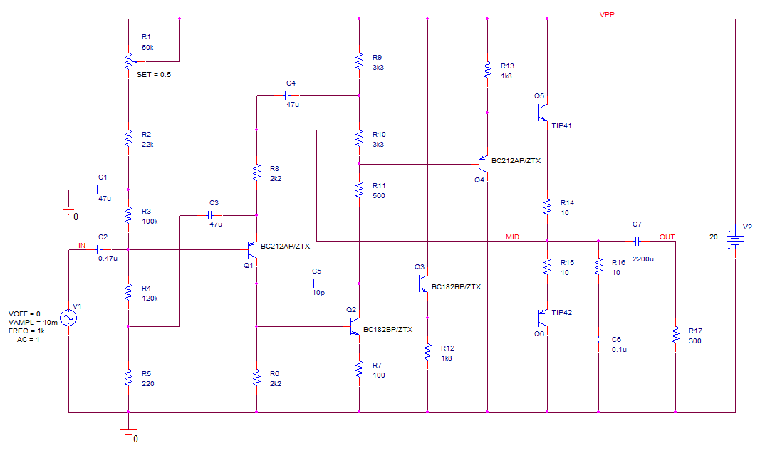
Now complete the schematic, as shown below. Place a VSIN part from the Source library, referenced V1 in the schematic image, and set the properties: VOFF to 0, VAMPL to 10m, FREQ to 1k and AC to 1; for information: this will provide a 10mV sine source at 1kHz for Transient Simulations and a 1V source for AC Sweep simulations, those are covered later. Place a VDC part from the Source library, referenced V2 in the schematic image, for the power supply, change the 0Vdc value to 20 for this circuit, PSpice will "know" that the value is a DC voltage so it is not necessary to specify V, or Vdc, with the value. Use Place>Ground from the menu to place the 0 symbol required for the PSpice reference, this is from the Capsym library. Then use Place>Net Alias and assign the IN, OUT and VPP Nets Aliases to the wires as shown. When placing the Net Aliases, control+E can be used to change the name on the cursor, rather than using Place>Net Alias three times.
Use File>Save from the menu to save the current schematic.
Now that the schematic has been completed, move on to the next section to look at simulating the design. Note that the schematic must be completed before moving on to the next section.
NEXT SECTION > "Simulating the Schematic"
Copyright © 2022, Parallel Systems Ltd.
All rights reserved.