3. Simulating the Design
This section describes how to use OrCAD© Capture-PSpice© to simulate the circuit for the Headphone Amplifier example design.
You will need to complete Section2: Entering the Schematic before you will be able to work through this section.
The sequence to run the simulations involves setting the Simulation Profile for the required simulation type and then running the simulation. The Simulation Profile can either be edited for each simulation, or a New Simulation Profile can be created, as required. The small advantage to having multiple Simulation Profiles is that it will then be possible to switch between the simulation settings without editing the Simulation Profile.
There are four basic simulation types for PSpice: Bias Point, DC Sweep, AC Sweep and Transient. The Bias Point simulation applies any DC sources and allows the circuit to get to a stable state. The other simulation types will start by running the Bias Point simulation, to get the circuit to a stable state, and then run the selected simulation type. A DC Sweep will apply multiple values to a Voltage, or Current, source, a Model Parameter, a Global Parameter, or Temperature. An AC Sweep will apply multiple values to any AC sources within the design, typically used to evaluate the frequency response of the circuit. A Transient analysis will evaluate a circuit in real time such that it will then be possible to view the waveforms within the circuit, similar to using a bench oscilloscope.
Bias Point Simulation
In this section, a Bias Point Simulation will be configured and run, from the menu either take PSpice>Edit Simulation Profile to edit the existing simulation profile; or take PSpice>New Simulation Profile to create a new simulation, this will need a name, like "runBias" for example.
Set the Analysis type to Bias Point, if required, the other default settings for the Bias Point will be fine for this simulation. Note that the name of the Simulation Profile, "bias" in this case, is shown in the heading for the Simulation Settings form.
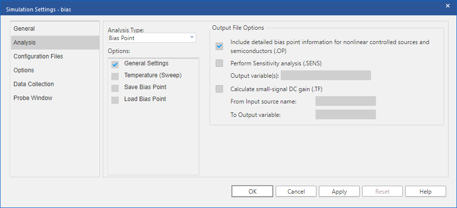
Left-click on OK to accept the Simulation settings and close the Simulation Settings form. Then, from the menu take PSpice>Run to run the simulation.
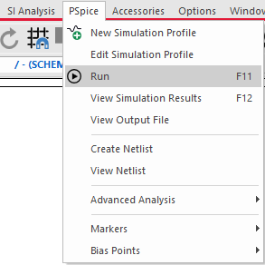
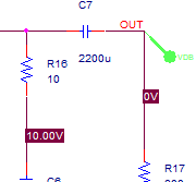
The simulation will then run and report any errors if the design check fails, if you get any, these will need to be investigated and rectified before proceeding with this section. The Probe window will be opened, you will see an icon for this on the Taskbar, but the Probe Window will be empty since the Bias Point Simulation will have generated a single result, just the stable bias values for the circuit. The Schematic will have been updated with the values from the Bias Simulation, activate the Capture Schematic window, if it is not already active, to view the schematic. Display of the Bias points is controlled by the circular V, I and W icons on the toolbar
![]()
If not already enabled, left-click on the VD icon to enable the display of the Voltage Bias values in the schematic. (The CD icon can be used to enable the Current Bias values in the schematic, and PD icon for the Power Bias values.) In the following screenshot Voltage and Current Markers have been enabled.
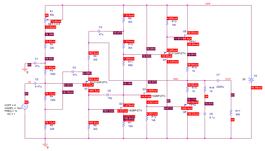
Check that the bias marker values are very close for your schematic, different voltage and current bias values may indicate that the circuit is connected incorrectly, or that the values are incorrect for some circuit elements. Due to automatic placement of the Bias Values in the schematic, it could be possible that some markers overlap giving the impression of larger values than could be possible with the 20V supply. If necessary, the Bias Values can be moved by left-clicking and dragging them, there will be a "dotted trail" from the marker to the net it is attached to once it is moved.
DC Sweep Simulation
From this point onwards, the circuit will need to be correct so be sure to correct any connection or circuit value issues before proceeding
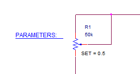
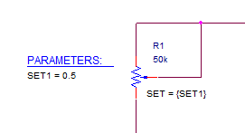
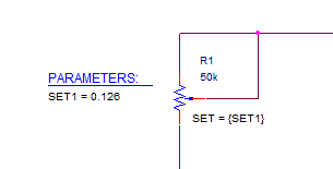
The first thing to correct is the output voltage. With the current values the voltage at the MID net is not set to the mid-point of the power supply, this may not have any adverse effect upon circuit performance but we can use PSpice to help to find the correct bias to set. At present, the set point, effectively the position, for the POT is set to 0.5, the middle of the range, a couple of simple changes will allow the set point (position) to be varied to find the required operating point. Use Place>Part from the menu and set the Part to PARAM, from the Special library, press enter to get this part onto the cursor and place the part towards the upper left of the schematic page, near the POT, as shown in the screenshot. Note that the actual position of the PARAM part in the schematic is not critical but since, in this case, the PARAM will only be applied to the set point for the POT, it makes sense to place it nearby.
Once the PARAM part is placed, the Properties can be edited and the new Property for the Parameter can be added. Double-click on the placed PARAM part in the schematic to open the property editor.
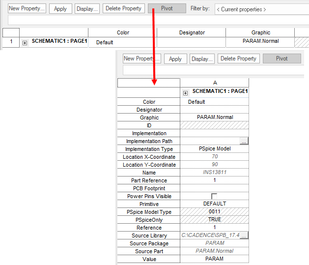
If necessary, use the Pivot button to pivot the Property Editor grid so that the properties are listed at the left-hand side of the tab, this will usually allow all of the Part Properties to be viewed without the need to pan, or scroll, through them.
Then add the new Property, left-click on the New Property button to get the New Proprerty form to open.
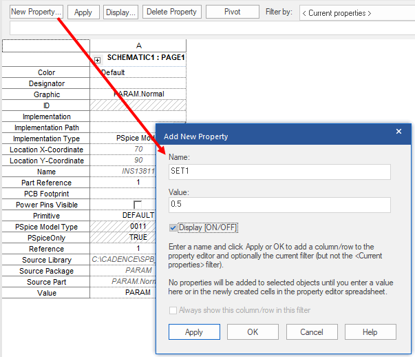
Set the Name of the new property to SET1 and the Value to 0.5, this will just be a default value for now, set the Display On / Off and left-click on OK to add the value.
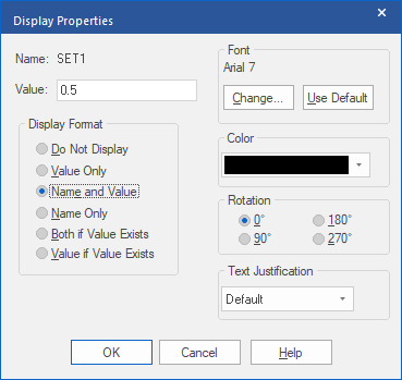
When the Display Properties form appears, set the Name and Value option and Left-click>OK. This will make editing the property easier by being able to double-click on the visible text and change the parameter value. (Having the parameter and value visible is not a requirement to get the simulation to run)
The resulting PARAMS part in the schematic.
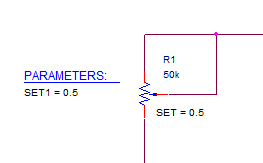
Next the parameter will be assigned to the SET property for the POT, double-click on the "SET=0.5" displayed property for the POT part, and change the Value for the SET property from 0.5 to {SET1} and left-click>OK to set the value to use the SET1 Parameter value, instead of a fixed value for the set point of the POT.
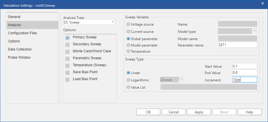
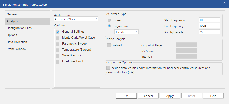
Now that the design has been setup to use a parameter for the setpoint of the POT, a DC Sweep Simulation Profile can be configured to sweep the setpoint of the POT to find the required value to set the output voltage to the halfway point of the supply voltage. Either use PSpice>New Simulation Profile, provide a new name for this Simulation Profile and set the Analysis Type to DC Sweep, or use PSpice>Edit Simulation Profile and change the Analysis Type from the current Bias Point to DC Sweep, in both cases, configure the Simulation Profile parameters as shown:
Then PSpice>Run to run the simulation and, when the Probe Window opens, use Trace>Add Trace and select the V(MID) entry, or add a Voltage Marker (PSpice>Markers>Voltage Level) to the MID net. Note that the OUT net goes through a capacitor so the voltage on that net won't reflect the change in Bias! From the Probe Window, note the point at which V(MID) is at 10V, half the supply.
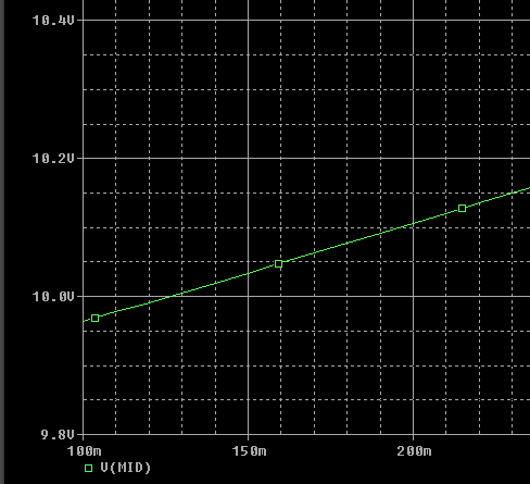
A "visual check" is not going to be too accurate but the PSpice Cursor function can be used to find the "exact" value.
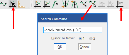
Left-click on the "pointer" icon to enable the cursor function, then left-click on the "magnifying glass" icon to open the Search Command, set the search command to "search forward level (10.0)", without the quotes, and left-click>OK. This will move the cursor along the X axis until the Y axis value is equal to the specified level. The Mark Label icon, rightmost icon shown above, can be used to display the cursor value on the Probe display.
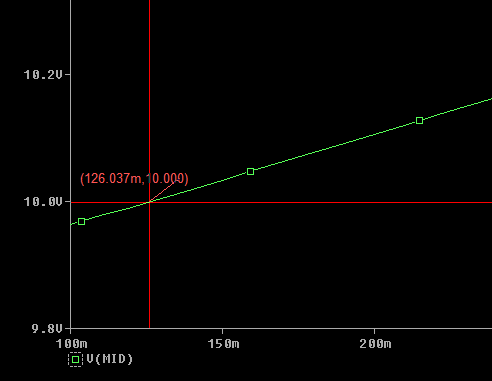
In this case, the marked value is 126.037m, or 0.126 will suffice. The value for your simulation may differ due to the POT having different connections, for example.
Double-click on the SET1=0.5 text for the PARAMETERS part property and set the value of the SET1 property to the value found for the 10V output, 0.126 in this case or, whatever you found for your circuit.
AC Sweep Simulation
Now that the circuit bias has been established, and AC Sweep can be run to determine the small signal frequency response, since the application is intended to be audio, the sweep will be set for 10Hz to 100kHz. Remember to use MEG as the multiplier if your frequency sweep needs to run to Megahertz!
Either use PSpice>New Simulation Profile, provide a new name for this Simulation Profile and set the Analysis Type to AC Sweep, or use PSpice>Edit Simulation Profile and change the Analysis Type from the current DC Sweep Point to AC Sweep, in both cases, configure the Simulation Profile parameters as shown:
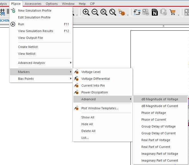
And then left-click>OK to accept the settings. This will run the sweep from 10Hz to 100KHz using 25 points per decade. Next place the DB Voltage Marker on the OUT net, PSpice>Markers>Advanced>dB Magnitude of Voltage. Delete the Voltage Marker from the MID net if you added one for the previous simulation.
Then run the simulation, PSpice>Run, the simulation will run and the the Probe Window will open with the frequency response at the OUT net shown. The Probe in the schematic will change to reflect the trace colour.
Transient Simulation
To complete the Analysis types, a Transient Analysis will be run and the output waveform checked.
Either use PSpice>New Simulation Profile, provide a new name for this Simulation Profile and set the Analysis Type to Transient, or use PSpice>Edit Simulation Profile and change the Analysis Type from the current AC Sweep Point to Transient, in both cases, configure the Simulation Profile parameters as shown:
![]()
This profile will run the simulation for 5mS, 5 cycles of the 1kHz input source, the Maximum Step Size setting forces the simulator to re-evaluate the circuit at least every 10uS to improve the resolution of the output. Place a Voltage Marker on the OUT net, if you edited the previous simulation profile, remove the DB Voltage marker first (select it and Delete), PSpice>Markers>Voltage Level. Then run the simulation, PSpice>Run from the menu. The simulation will run and the the Probe Window will open with the waveform at the OUT net shown. Again, the Probe in the schematic will change from grey to reflect the trace colour.
![]()
Now that the schematic has been completed, move on to the next section to look at laying out the physical design. Note that it is recommended that you simulate the circuit before moving onto physical layout to check that the circuit has been entered correctly.
NEXT SECTION > "PCB Physical Layout"
Copyright © 2022, Parallel Systems Ltd.
All rights reserved.