* This next part of the tutorial assumes that you have completed all the steps in the previous sections
Entering the schematic and Simulating the circuit please go and complete these before attempting this next step *
4. Physical Layout
Before we start making the design ready for PCB Layout we need to make a few changes to the schematic. We need to add the connectors as shown in the initial preview of the design and we also need to add a property to the load resistor so that it is ignored by the netlist and hence not in the PCB Layout.
Add the connectors J1-J3 by using the Place>Part command, add the Connector library from C:\Cadence\SPB_17.4 then tools\Capture\library and then locate the HEADER2 part and place it three times. You may need to use right-click>Mirror Geometry or the right-click>Rotate command to get the orientation to match the original schematic.
Next we need to ensure that the load resistor R17 is ignored by the netlist. This part has only been added to aid in the PSpice simulation and is not required for the actual design, the load will be the "headphones". Double-click the part R17 and then left-click on New Property and add a new property Name of PSpiceOnly with a Value of TRUE.
Use File>Save to save the design.
Next the PCB Footprint property values need to set for all of the parts in the design. These values assume that the default PCB Footprints from the product installation are being used, IF your installation is not configured to use the default PCB Footprints from the product installation, you will need to specify PCB Footprint property values for the names of the footprints that match the footprints in your libraries. Also note that there will need to be an exact match between the numbered pins in the schematic part and the numbered pins on the PCB Footprint.
There are several ways to specify PCB Footprints for parts in the Cadence tools. The recommended way is to use OrCAD Capture CIS which allows the property information (like PCB Footprint, Manufacturer etc.) to be stored in a Windows compliant ODBC database like Microsoft Access or an SQL database. If you are using this flow then the properties do not need to be added manually as we will show in the next few steps. We will show two methods to assign a PCB Footprint.
1. Select the part J1 and then right-click>Edit Properties to launch the Property Editor (you can also double-click part J1 to bring up the same Property Editor).
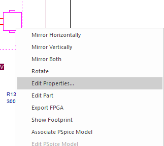
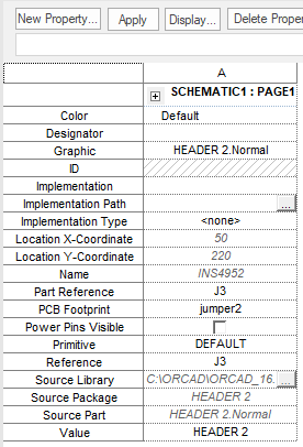
2. Enter a value for the PCB Footprint property for J1 in the appropriate cell. In this example the PCB Footprint is called jumper2, you only need to specify a PCB Footprint name, no extensions are required.
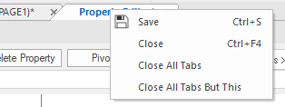
3. Save the changes and close the Property Editor. One method is to right-click on the Property Editor tab, Close.
You can apply other properties to parts using this method like Manufacturer, Part Number, and Tolerance etc. Properties on parts are used to create PCB Editor Netlist files and manufacturing data like a Bill of Materials. A second method to add many properties in one step is to use the Browse method.
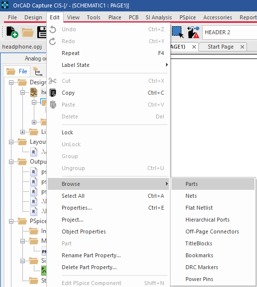
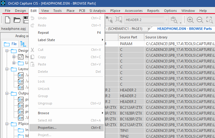
4. Select the headphone.dsn in the project window then Edit>Browse>Parts
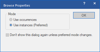
5. Accept the message about the property preferred mode. (For further information on Instances vs Occurrences properties please refer to the OrCAD Capture User Guide).
6. You will now see a list of all the parts in the Capture design. We only need to be concerned with the parts that will be used for the Physical layout. We can ignore the PSpice parts so, left-click C1 followed by a shift+left-click R16, the rows will highlight
7. Choose Edit>Properties (or CTRL+E) to launch the Browse Spreadsheet window. This is an editable table where you can edit existing property values or add new Property values like Manufacturer, Part Number that will be used for the Bill of Materials.
8. Locate the PCB Footprint column and enter the following values for PCB Footprint:-
| RefDes | PCB Footprint | RefDes | PCB Footprint |
| C1 | smc0805 | R1 | resadj |
| C2 | smc0805 | R2 | smr0805 |
| C3 | smc0805 | R3 | smr0805 |
| C4 | smc0805 | R4 | smr0805 |
| C5 | smc0805 | R5 | smr0805 |
| C6 | smc0805 | R6 | smr0805 |
| C7 | smc1210 | R7 | smr0805 |
| J1 | jumper2 | R8 | smr0805 |
| J2 | jumper2 | R9 | smr0805 |
| J3 | jumper2 | R10 | smr0805 |
| Q1 | to236ab | R11 | smr0805 |
| Q2 | to236ab | R12 | smr0805 |
| Q3 | to236ab | R13 | smr0805 |
| Q4 | to236ab | R14 | smr0805 |
| Q5 | to252aa | R15 | smr0805 |
| Q6 | to252aa | R16 | smr0805 |
9. Left-click>OK to close the Browse Spreadsheet and right-click>Save and then Close on the Browse tab to save the property edits.
10. Select the headphone.dsn in the Project Window and choose File>Save to save the design.
Design Rule Checks
After you have completed your design, it is recommended that you run a design rule check (DRC) to isolate any unwanted design errors that might be there. To run a DRC on the headphone design complete the following steps:-
1. In the Project Manager window select the design file headphone.dsn.
2. From the PCB menu select Design Rules Check
3. In the Design Rule Check dialog box, the Design Rules Check tab is selected by default. Specify your preferences.
4. To run the DRC, select the Check design rules option button under Action and left-click>Run.
The DRC report is generated. To view you can either look at the Session log or access the report from the Outputs folder of the Project
Window. A sample section is shown below
********************************************************************************
********************************************************************************
--------------------------------------------------
Checking Schematic: SCHEMATIC1
--------------------------------------------------
Checking Electrical Rules
Checking For Single Node Nets
Checking For Unconnected Bus Nets
Note that a DRC Warning will be flagged for the PARAM part in the Schematic. As this part has no Pins, the "Check device with zero pins" batch DRC option gets this warning issued. This DRC Warning can be ignored as it won't have any impact on any subsequent steps
Creating a PCB Editor Netlist
1. In the Project Manager window select the design file entry headphone.dsn.
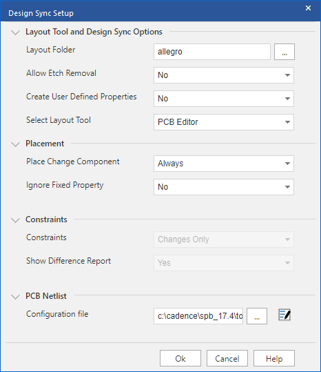
2. From the PCB menu select Design Sync Setup, the default settings should be fine so, left-click>OK
3. Then, from the PCB menu, select New Layout
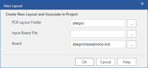
4. Check that the Input Board File is empty to create a board with a default template and left-click>OK
5. If you see the Cadence 17.4 ALLEGRO Product choices, pick an OrCAD PCB Designer Standard, or OrCAD PCB Designer Professional, license.
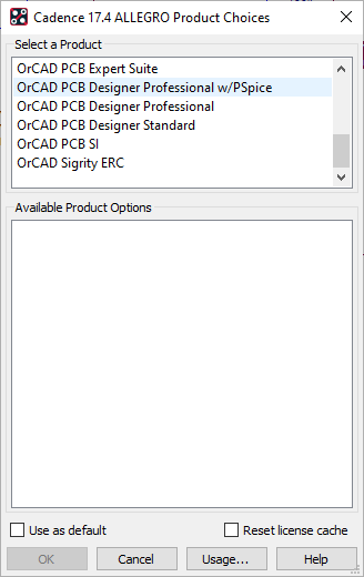
6. Left-click>OK.
The board file, headphone.brd opens in OrCAD PCB Editor.
Capture can be closed at this point, "Yes All" to save any changes.
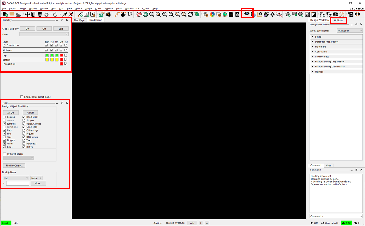
Details of the highlighted items are illustrated in the following screenshots:
Co-ordinates view and Units in the Status Bar![]()
![]() Show Element (F4) Lists the attributes of the item selected
Show Element (F4) Lists the attributes of the item selected
Options pane: This changes depending on the command being used
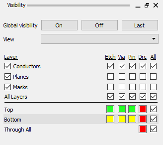
Visibility pane: This provides access to "quickly" controls visibility, "all" colour and visibility control is available through Setup>Colors
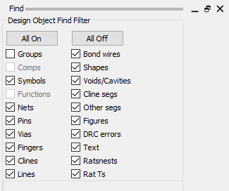
Find pane: This controls what can be selected in the PCB design canvas, restricting "what" can be selected.
For more information about OrCAD PCB Editor please refer to the PCB Editor User guide, available from Help>Documentation menu.
Setting up PCB Editor
These next few steps will guide you through some basic settings inside PCB Editor to suit your design environment.
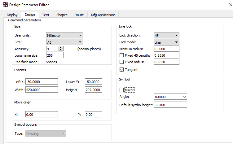
1. Setup>Design Parameters, Design tab
2. Set the user units to Millimeter, the Size to A3 and Left X and Lower Y to -50.
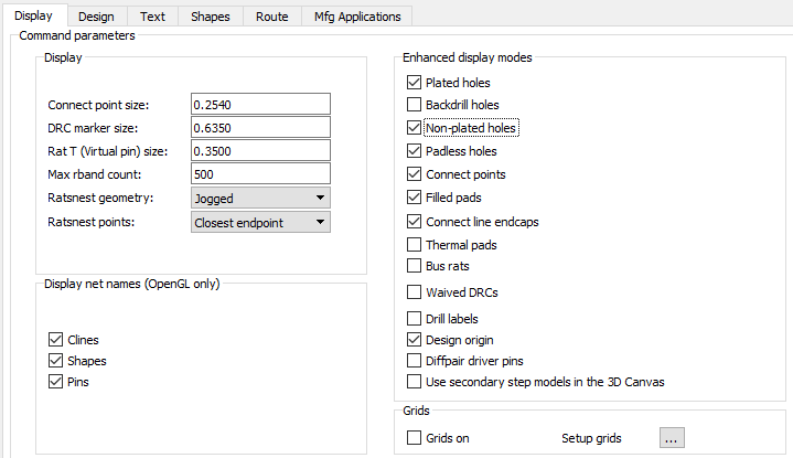
3. Go to the Display tab and enable the display settings as shown below
4. Left-click the "..." icon to the left of Setup grids and set the grids as follows:
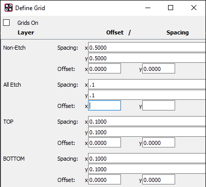
Placement will then be on a 0.5mm by 0.5mm grid and routing will be on a 0.1mm by 0.1mm grid, use the "All Etch" entries to set all of the Etch (routing) grids to be the same.
5. Left-click>OK to save the settings.
Creating a board outline
The board outline (or Design Outline) defines the boundary of the PCB. This can be used for ECAD-MCAD Transfer using IDF/IDX as well as exports such as IPC2581. To create a board outline in PCB Editor.
1. Shape>Rectangular (Although Polygon and Circle can also be used).
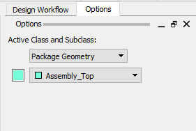
2. Set the Options menu as follows for Class and Subclass (layers in PCB Editor).
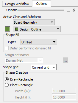
3. In the command window type x 0 0 followed by a return which will start drawing the rectangular shape from the co-ordinate 0,0.
4. In the command window type x 50 30 followed by a return to complete the rectangular shape at the co-ordinate 50,30.
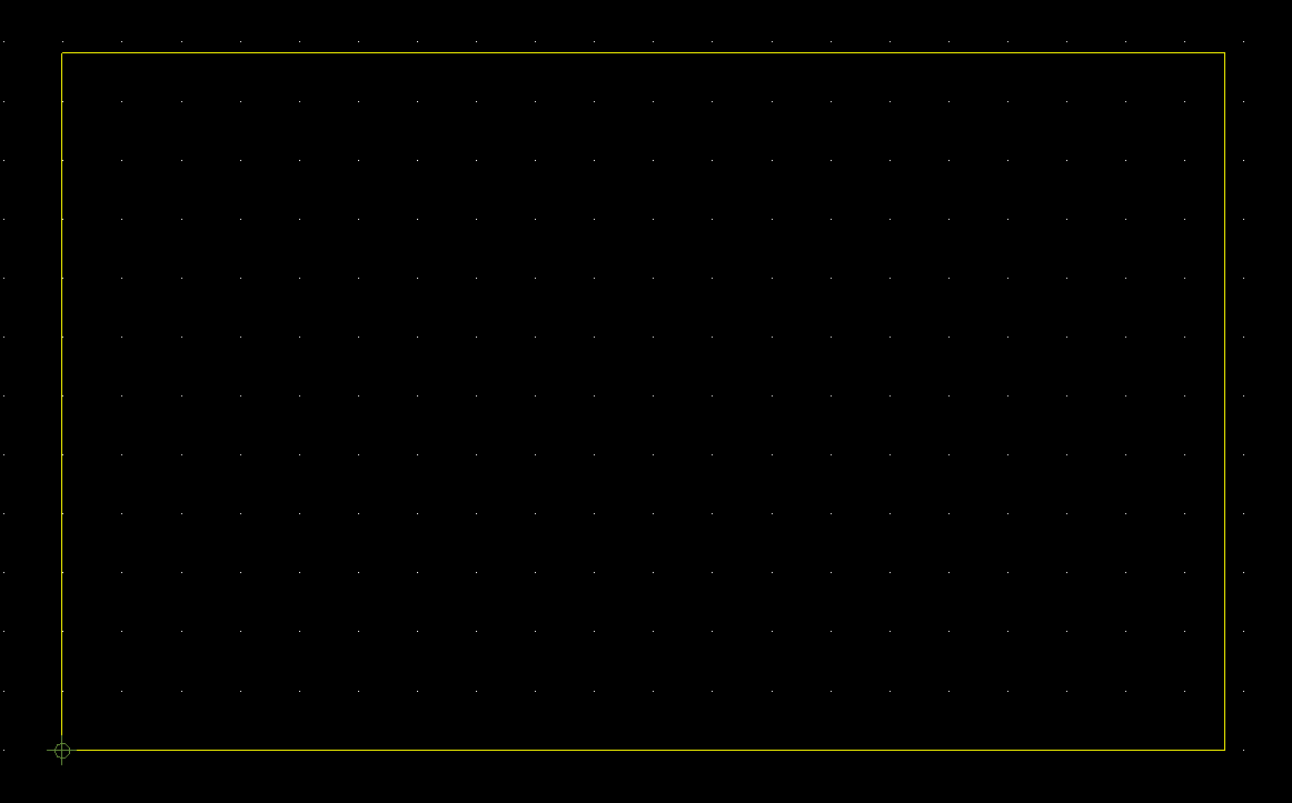
5. Right-click>Done (or F6) to end the active command.
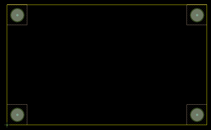
6. You have now drawn a PCB outline that is 50mm in the X and 30mm in the Y.
7. Tip: To delete the outline either hover over it until it highlights then right-click>Delete or invoke the Edit>Delete command then left click the shape to delete it followed by a right-click>Done.
8. Select Display>Zoom>Fit (or press F9, or use the icon ![]() ) to centre the board outline in the design window.
) to centre the board outline in the design window.
If required you can adjust the colours of the layers (called Classes and Subclasses). To do this:-
9. Setup>Colors
10. Select Geometry and then choose a colour in the bottom of the pane then select the coloured swatch next to the subclass you wish to change (In this example choose Yellow and then choose the Design Outline). Any changes are made dynamically so your design outline will change to Yellow. (This change was already made in the screen shot above)
11. Left-click>OK to close the Color Dialog.
Adding Mounting Holes
Now that we have a board outline, let's add some mounting holes to the PCB. To do this:-
1. Place>Mechanical Symbols. You'll see a list of default Mechanical Symbols to choose from.
2. Since we want to place 4 of these symbols, select the Advanced Settings tab.
3. Change the AutoNext from enabled to Disable then select the Placement List tab.
4. Select the required mechanical symbol. For this tutorial choose MTG125
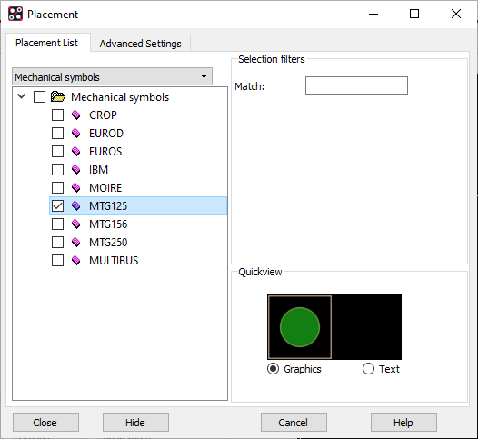
5. Left-click>Hide.
6. The Placement dialog closes and the mechanical symbol MTG125 is attached to the cursor ready to place.
You can either left-click to place the tooling hole at the required location or type the x/y co-ordinates in the command line to place the tooling hole at the required location. For this example we will enter the co-ordinates.
7. At the command line enter x 2.5 2.5 followed by a return, the first tooling hole is placed.
8. Place the next three symbols at x 2.5 27.5, x 47.5 27.5 and x 47.5 2.5.
9. Right-click>Done to end the mechanical symbol placement.
10. File>Save to save your board design, left-click>OK to "Overwrite?"
Note: Alternatively, you can select Copy from the Edit menu and then left-click the first placed mechanical symbol. The selected mechanical symbol is now attached to your cursor ready for placement, right-click>Done to end the copy command. Another method is to hover over the symbol and choose right-click>Copy
Placing Components.
After you have created the board outline and placed the mounting holes you can start to place the components in the board. OrCAD PCB Editor supports both manual and auto placements. For manual placement you can also place parts directly from the schematic or via a ROOM property specified in OrCAD Capture. Although these are not covered in the tutorial please take a look at the following How To Videos: - http://www.youtube.com/watch?v=OoaR8KixmBs?rel=0 and http://www.youtube.com/watch?v=si_FFID2C6I?rel=0
In this section we will use manual placement to create the PCB for the headphone design. There are different ways in which you can select a component for placement. In this tutorial you will learn to place components by refdes only.
1. From the Place menu, select Components Manually.
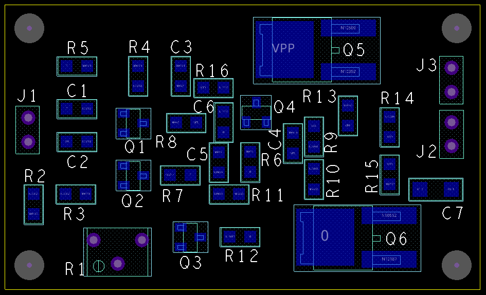
The Placement dialog box appears showing in a collapsing tree view all the components that you can place in your design. For example for this tutorial the components are C1-C7. J1-J3, Q1-Q6 and R1-R16.
Note: Only unplaced components are displayed in the Placement form when opened. The "cyan" icons change to "green" with a "P" once parts are placed.
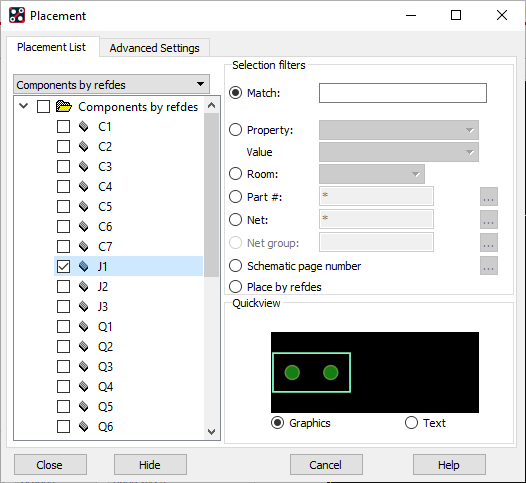
2. Select the J1 component by clicking the check box next to the component name as shown in the figure above.
Note: You can also select all the components of a type by clicking the check box next to the folder icon
Note: The Quickview window displays the footprint shape for the selected component in graphics and text mode.
3. Left-click>Hide. The Placement dialog box closes and the component (in this case J1) that you have chosen is attached to the cursor.
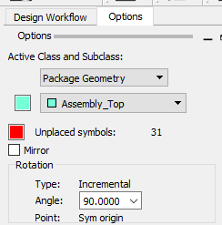
4. Move the component to the desired location. You can use right-click>Rotate to rotate in either direction and at any angle set by the Options fold out menu Rotation angle setting.
5. Left-click once the desired rotation is set and left-click to place at the required location. You can also use the x/y co-ordinates as you did earlier with the tooling holes or if you have a marker point (like a crosshair from a DXF import) use the hover, right-click>Snap Pick to>Intersection.
Note: During placement there are also right-click>Mirror which will place the component on the other side of the PCB, Top to Bottom, or Bottom to Top, if required, for double sided assembly.
6. Using the techniques you have used place all the components from the available components list. A sample placement is shown below.
7. Select Display>View>Refresh to refresh the screen, or press F5.
Tip: To Find a component in PCB Editor.
In the Find Filter (Panel on the right hand side of the screen)
Select Comp (or Pin) option from the Find by Name drop down list, left-click>More, the Find by Name Property dialog box appears displaying all available components.
Select a component that you want to find. The selected component appears in the selected object grid, left-click>OK, the component is highlighted in the design window.
Similarly, you can find net(s) or symbol(s) in PCB Editor. To find a net, select the Net option from the Find by Name drop down list. You can also select the symbol or net in the schematic and PCB Editor will zoom and centre in on the net or symbol.
Design Rule Checking
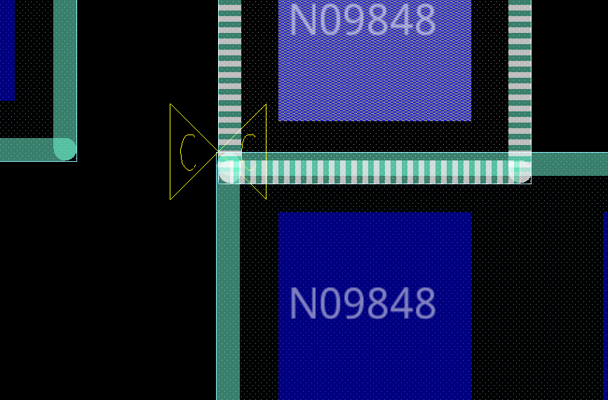
PCB Editor allows you to run DRC online (On) or in batch mode (Off). The default is On. While placing the components if there are any design rule violations, then error markers are displayed on the board. An example of a Placement DRC (C-C) is shown below.
Note: To run DRC online, select the Enable On-Line DRC from the Setup>More menu.
Setting the Design Constraints
To configure the basic spacing and physical constraints for your board design, select Setup>Constraints. A window appears showing the default settings. For this tutorial, we will accept the default values apart from the default line width. To set this:
1. Setup>Constraints. This launches Constraint Manager.
2. Select the Physical tab.
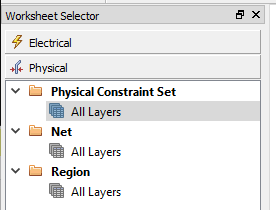
3. Select the worksheet Physical Constraint Set, All layers to open the physical rules.
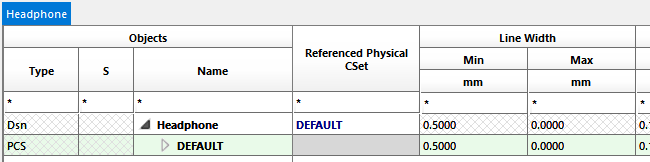
4. Change the value for the DEFAULT rule for Min Line Width from 0.127 to 0.5.
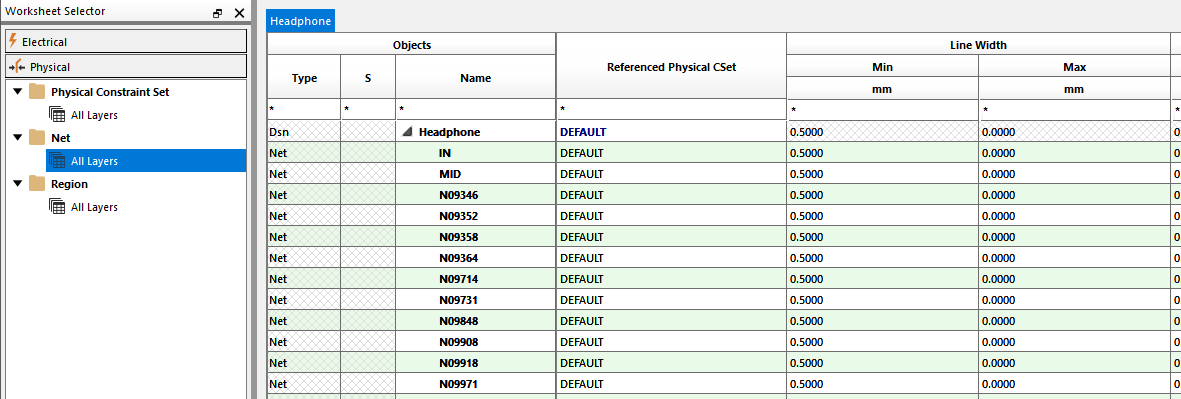
This sets the DEFAULT rule for all nets to use a 0.5mm track. To verify:-
5. Select the Net, All Layers worksheet to see the updated value.
For further information on setting physical and spacing constraints please watch: - Cadence PCB Physical Constraints - YouTube and Cadence PCB Spacing Constraints - YouTube
Routing
After completing the board placement, you can route the headphone board to complete the electrical connections between components.
OrCAD PCB Editor supports both manual routing and Auto-routing. The general use model is to first route any critical nets manually, lock them and then autoroute the rest of the board but this is user specific.
Manual routing
The steps involved in the manual routing process are as follows:-
- Check the board outline, via definitions, routing and via grids.
- Route power and ground
- Fan out surface mounted devices and verify connections to power and ground.
- Route the remaining signals using the manual routing tools.
- Optimise routing using the manual routing commands.
- Check for route spacing violations and check routing statistics.
Note: To know more about each of these steps, please refer to the PCB Editor documentation.
Manually routing VPP and GND (0) nets
1. Select the Assign Colors> command (Display>AssignColors) and pick a colour from the Options menu
2. Select the Net option from the Find By Name drop down list.
3. Left-click More, the Find by Name or Property dialog box appears displaying all available nets.
4. Select VPP, the VPP item appears in the Selected objects grid.
5. Left-click>OK, All VPP nets are coloured the selected colour in the design.
6. Select Connect from the Route menu.
Note: Alternatively, you can press F3 or click the icon ![]()
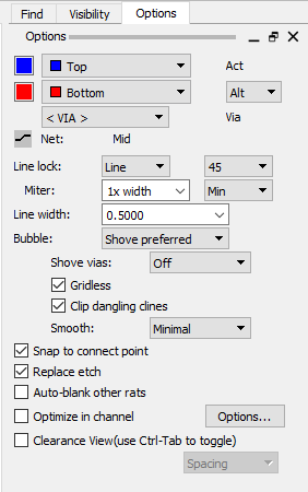
7. Left-click on the net to be routed, you can adjust the route settings from either a right-click or look at the Options tab.
8. Draw the net through the desired path.
9. When you have completed routing, right-click on the net and select Done.
Similarly perform the above steps for manually routing the GND nets.
Manually routing the remaining nets
1. Press the ![]() icon to fit your board in the design window.
icon to fit your board in the design window.
2. Place the cursor on the net to be routed and press F11 or ![]() icon to zoom in. You can also scroll your mouse wheel to zoom in / out or click and hold the centre mouse wheel to pan.
icon to zoom in. You can also scroll your mouse wheel to zoom in / out or click and hold the centre mouse wheel to pan.
3. Select Connect from the Route menu or Press F3. The Options panel changes.
4. Left-click on the net to be routed. The Options panel changes again to show the selected net as shown below
5. Draw the net through the desired path.
6. When you have completed routing, right-click on the net and select Done.
To change layers whilst routing (add Vias).
1. Left-click on the net to be routed.
2. Route to a point where you want to add a via, right-click on the net and select Add Via (or double-click the left mouse button). A via is added. The current Active layer becomes the Alternative layer and vice versa. For example if you have a Top and a Bottom layer, where Top is the current Active Layer, then when you add a Via the Bottom layer will become the Active layer and the Top layer becomes the Alternate layer.
3. Draw the net through the desired path.
4. When you have completed routing, right-click on the net and select Done.
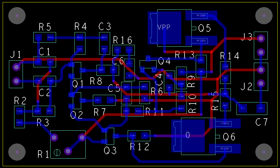
For this tutorial, a routed example of this board is shown below.
Autorouting within PCB Editor
OrCAD PCB Editor supports auto routing of all, or selected, Nets. The board will need a Shape added to the Board Geometry / Route Keepin class to restrict the routing area for the autorouter. See the next section on adding Shapes to the board.
And for more information, see the PCB Editor documentation.
Adding a Copper Shape to the Bottom Layer.
This section will add a single copper shape to the Bottom Layer by copying and "shrinking" the design outline. Copper shapes can be used in place of routing, for example the GND (0) routing on the bottom side of the PCB may give better screening results if the complete side of the PCB were a copper shape.
Note: If the design intent was to use a copper shape you would not need to manually route the (0) net. A copper shape, once assigned to the net (0) will consume the ratsnets.
1. From the Setup menu select Colors.
2. In the Colors dialog set Global Visibility to Off to turn off all the layers.
3. Go to Stackup folder in the left hand tree control and then left-click>All for Bottom, this will turn on all the colours for the Bottom layer.
4. Next choose the Geometry folder and turn on the Design_Outline colour to enable the colour for the design outline.
5. Left-click>OK to close the Color dialog.
6. From the Outline menu, select Z-Copy. (Or use Shape>Z-Copy)
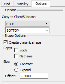
7. In the Options tab, pick ETCH and Bottom as the target Class/Subclass, then left-click on the Create Dynamic Shape box to create a Dynamic Shape, left-click on the Contract button and specify 0.5 as the contract amount. (required distance from board edge to copper shape).
8. Move the mouse to the main canvas area and left-click on the design outline to copy it, then right-click>Done.
9. From the Shape menu, choose Select Shape or Isolation/Cavity and left-click the shape just created, it will highlight.
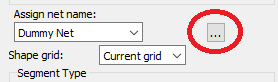
10. In the Options tab left-click the "..." button to the left of the Assign net name box and then choose 0 from the list of nets displayed. left-click>OK to close the list of nets and right-click>Done to apply the net to the shape.
In the resulting shape, the 0 trace added will be merged with the 0 shape just added. If required the 0 connect lines could be removed since the shape is now providing connectivity.
Note: The Thermal relief connections and other shape settings are controlled from the Shape>Global Dynamic Parameters menu.
Adding a Shape Manually
11. From the Shape menu choose Polygon.
12. Set the Options tab to look like
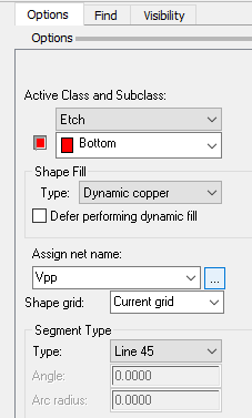
13. Draw a copper shape for the net VPP, you can either use the embedded net names to locate the net or the Assign Color command you used earlier to locate the pins / vias that form part of this net.
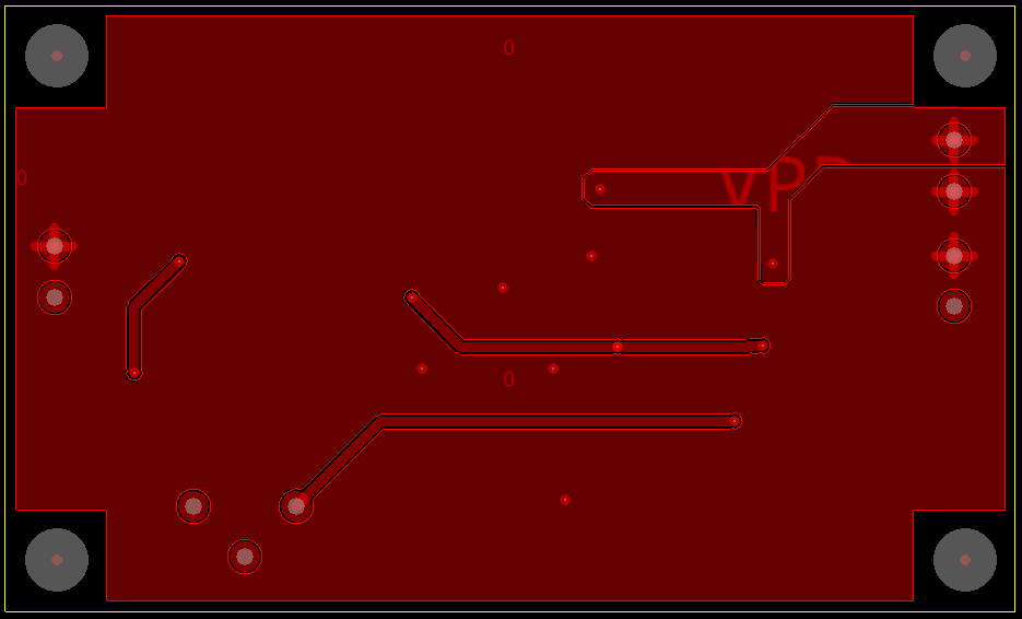
Your Bottom side should now look something similar to:-
Checking and reviewing the PCB
There are many ways to review your design once complete. A quick design check is to ensure that all the components are placed and routed.
1. From the Check menu select Design Status.
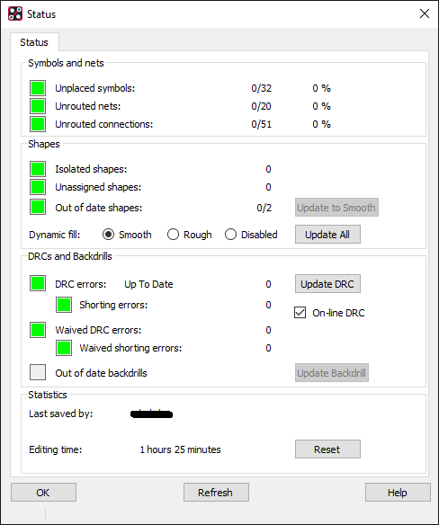
This is a summary of your design. Some of the coloured swatches will generate reports to give you further details on the status of your design. This is a good place to ensure that your design is complete and ready for post processing.
You can also run a variety of Reports giving information about your design. To do this:-
2. Export>Quick Reports>Summary Drawing Report. A summary of your design is listed in an html report.
There are many reports to choose from but you can also generate your own. For further information please take a look at: - https://www.youtube.com/embedEsrQQqMlUEE?rel=0
Post Processing
This section introduces some of the tasks that are not part of the placement and routing processes, but are related and can be performed using OrCAD PCB Editor. To know more about post processing, see the PCB Editor documentation.
Renaming components manually
After you have completed the placement and routing of your PCB, you can rename the components manually on the PCB in a specific order.
1. Set the Colours using the techniques you learned earlier so that you are displaying the following layers, Geometry\Design_Outline, Geometry\Assembly_Top, RefDes\Assembly_Top and Pin\Top.
2. From the Edit menu, select Text.
3. Left-click the reference designator you want to modify. The selected reference designator appears in the command line.
4. Change the reference designator as required in the command line and press the Enter key.
PCB Editor renames the component. The reference designators for the component on the board changes.
Note: PCB Editor will not allow you to have identical refdes so for example if you rename R5 to R6 and R6 already exists the resistor that is R6 will be renamed to R5.
Automatic renaming of components.
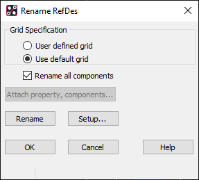
1. Select Manufacture>Auto Rename Refdes>Rename
. The rename refdes dialog appears.
2. Select the Use default grid option button. This option uses the default grid, which constitutes an internal method of renaming components.
3. Left-click>Setup, the Rename Refdes setup dialog box appears on which you set all the reference designator parameters.
4. Remove the T and B from the Top and Bottom Layer Identifier (this setting would add a T to each refdes for Top placed components and B for Bottom placed components. With it blank the default refdes will be used.
5. Also check the box to Preserve Current Prefixes, to ensure the current used prefixes are used.
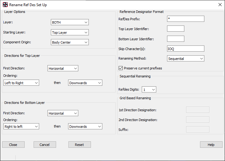
6. Left-click>Close to accept the settings and return to the rename refdes dialog.
7. Left-click>Rename in the rename refdes dialog box. PCB Editor automatically renames every component on your design in a single operation. The status of the renaming operation is displayed in the command line.
8. Save the board file (File>Save). We will use this board file to back annotate the component renaming to the schematic.
Back Annotation
While creating a PCB, you might make some changes in the PCB Editor board (.BRD) file. As a result, the board file and the design file in Capture may be out of sync. To ensure that both these files are in sync, you can back annotate the changes in the PCB file to OrCAD Capture.
When you back annotate, information, such as pin and function swaps and component names (changed due to renaming) gets added on to the schematic in OrCAD Capture.
To back annotate the changes to the schematic:
1. Open the headphone.opj in OrCAD Capture.
2. In the Project Manager window, select headphone.dsn.
3. From the PCB menu, select Update Schematic.
4. When the Update Schematic form appears, the list of changes are displayed, the components references in this case.
(Your list of changed references may differ from the screen shot)
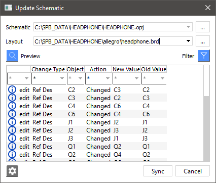
5. Left-click>Sync
The schematic is updated with the changes made in the board.
Schematic Changes
Similarly, if the board file is open in PCB Editor and you make changes in the schematic design, these changes will be forwarded to the board during netlist creation in Capture.
To do this:-
1. In the Project Manager window, select the headphone.dsn.
2. From the PCB menu, choose Update Layout. like the Update Schematic, any changes will be listed.
3. Left-click>Sync
Cross probing and cross highlighting between PCB Editor and OrCAD Capture
OrCAD PCB Editor is tightly integrated with OrCAD Capture. As a result, you can use cross probing to verify information flow between the schematic and the board design, and vice versa.
Cross probing lets you select an object in the OrCAD Capture schematic and see the corresponding object in PCB Editor.
To enable cross probing, Intertool Communication must be enabled. This is enabled by default but you can check this as follows:-
1. In the Project Manager window in OrCAD Capture, select headphone.dsn.
2. From the Options menu, select Preferences.
3. Left-click the Miscellaneous tab.
4. Ensure that the Enable Intertool Communications check box is selected in the Intertool Communication section.
5. Left-click>OK.
Before you start cross probing, tile OrCAD Capture and PCB Editor windows on a single screen or have them open on separate screens. Select a component in OrCAD Capture, PCB Editor automatically zooms and centres the corresponding component.
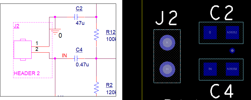
For example, if you selected J2 in the headphone.dsn file, the corresponding connector J2 will be displayed in PCB Editor as shown below:-
Cross highlighting lets you select an object in PCB Editor and see the corresponding object highlighted in OrCAD Capture.
In the case of cross highlighting between OrCAD PCB Editor and OrCAD Capture, just select a component in PCB Editor and the corresponding component will be highlighted in OrCAD Capture.
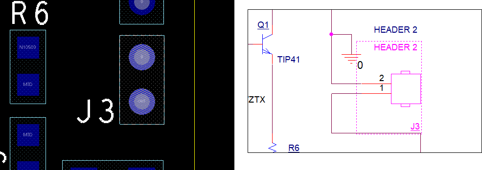
For example, if you select J3 in the headphone.brd file, the corresponding connector J3 will be highlighted in OrCAD Capture as shown below:-
Generating Output files.
The final task in creating a board design is to generate output files for manufacturing. You can create Gerber files, Excellon NC Drill files, DXF files, IPC2581, ODB++ as well as printer/plotter files. For a full list of possible exports explore the Export menu inside PCB Editor.
Note: before generating any output files, make sure your design status is up to date as we did earlier. If you need to review this please refer to "Checking and reviewing the PCB".
Using OrCAD PCB Editor, you can generate various files that can be further used by third party fabrication and manufacturing tools. To generate some of these output files, complete the following steps:-
1. From the Export menu, select Gerber Parameters, the Artwork Control form appears.
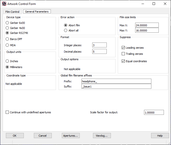
2. Select Gerber RS274X under the device section. Extended Gerber is the most standard Gerber format used today by most PCB Fabricators.
3. Set the Format for Integer and Decimal places to 3 and 5. (Supports output values up to 999.99999 mm)
4. Optional: Set a Prefix and Suffix like jobname- and -Issue1. This way your artwork film names will include the jobname, headphone in this case, and issue. You can then standardise on a film name (like TOP, BOTTOM, SPTOP, SMTOP), when your artwork film is generated the film will be called jobname-TOP-Issue1.art, and so on.
5. Accept the remainder of the default settings and left-click>OK to close the Artwork Control form dialog box.
6. From the Setup menu, pick Colors then left-click on the Off button for Global Visibility. This turns all layers off.
7. From the Stack-Up folder turn on the colours for Pin Soldermask_Top, the Soldermask layer is turned on. (If desired, add Via / Soldermask_Top to "open" the Vias)
8. From the Geometry folder select All for Soldermask_Top which will also turn on both Board and Package Geometry Soldermask_Top layers.
9. Select Gerber from the Export menu, on the Film Control tab, mouse over the TOP film entry and right-click>Add. Specify the new film name as SMTOP and then left-click OK to add the new film.
10. Repeat steps 5-9 to generate new film for:-
SPTOP (Pastemask_Top) with Pin / Pastemask_Top and Package Geometry / Pastemask_Top.
11. Close the Color Dialog form.
12. In the Artwork Control form, Film tab left-click on Select All to select all the films configured for this design
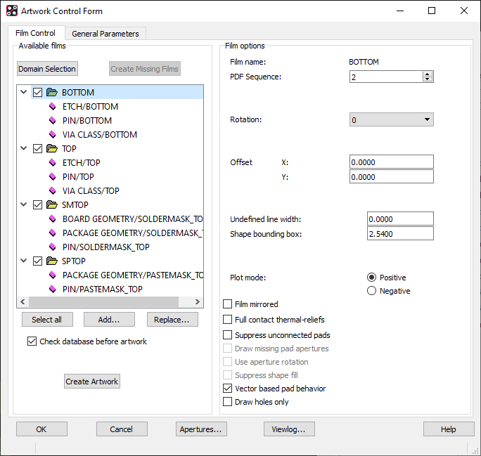
13. Left-click on Create Artwork. A message box appears showing the progress of the artwork creation, after the artworks are generated the artwork films with an .ART extension are saved under the headphone\allegro design directory (for this tutorial only).
14. Left-click>OK to close the Artwork Control Form dialog box.
NC Drill Data
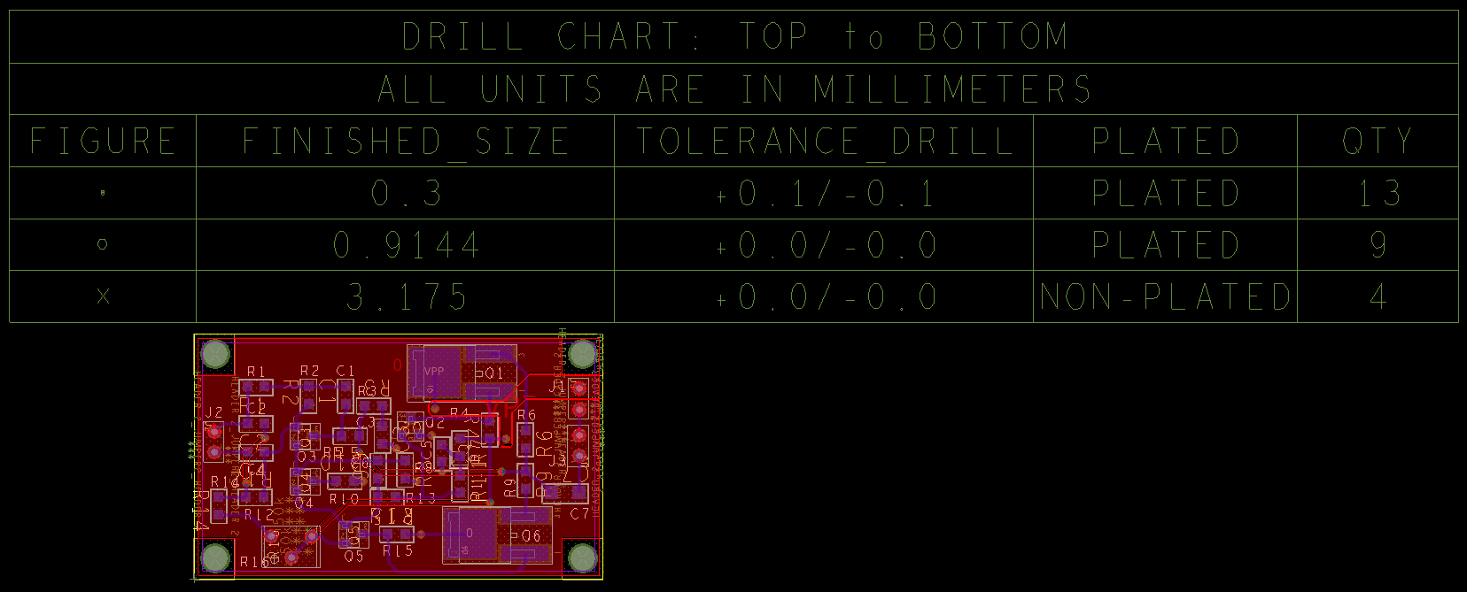
Next the Excellon NC drill data will be created. First, add the Drill legend to the PCB.
1. From the Setup>Colors dialog box turn the Global Visibility On then left-click>OK.
2. From the Manufacture menu, choose Create Drill Table and OK the resulting form. The drill legend symbol will then be attached to the cursor in the design canvas. Left-click to place the drill legend rectangle.
Now create the drill file.
1. From the Export menu pick NC Drill. The NC Drill form opens.
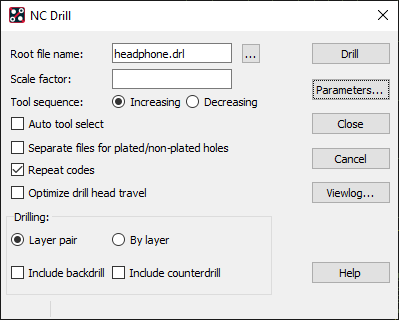
2. Left-click on the Auto tool select check box.
3. Left-click on NC Parameters.
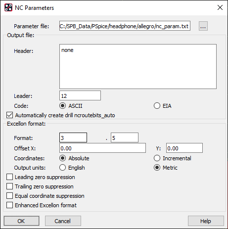
4. Enable the Enhanced Excellon Format check box.
5. Left-click on the Close button to close the form.
6. In the NC Drill dialog left-click on Drill to generate the drl file.
7. Left-click on the Close button to close the NC Drill form.
Viewing Gerber Data
You can view the artwork files that you created in PCB Editor.
Important: Only Cadence generated artworks are supported for viewing inside OrCAD PCB Editor.
To view the artwork:
1. From the File menu, select New and specify a new board file name of artwork.
2. Left-click>OK and left-click>OK on the New Drawing form.
3. From the Setup menu choose More>Subclasses.
4. Check the box next to MANUFACTURING.
5. Enter artwork for a new subclass.
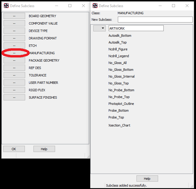
6. Left-click>OK.
7. From the Import menu, select More>Artwork.
8. Set the Class to Manufacturing and the Subclass to Artwork.
9. Using the "..." button next to filename, browse for the name of one of the artworks you wish to load.
10. Left-click>Load File. A dynamic rectangle that represents the extents of the Gerber data appears in the UI work area.
11. Left-click to place the artwork in the design window. The artwork is placed.
12. Repeat steps 9-11 to place other artworks as required.
Copyright © 2022, Parallel Systems Ltd.
All rights reserved.