
All content Copyright 2022 Parallel Systems Ltd.
1. Start (Windows Icon) >Cadence PCB 17.4-2019>Capture CIS 17.4
2. If the Cadence Product Choices appears, select a license that contains PSpice, like OrCAD PSpice Designer, or OrCAD PCB Designer with PSpice and so on.
(You may also see an OrCAD Capture CIS Option added to some selections, this adds the OrCAD Capture CIS functionality to the OrCAD Suite licenses that have just OrCAD Capture included.)
3. Choose File>New>Project to launch the New Project wizard.
4. Type RC in the Name field.
5. Use the left-click the “…” button for Location and navigate to the C:\OrCAD_Training\PSpice directory. (Or where you saved the training files)
Your new project is created and saved in this directory.
6. Left-click the Enable PSpice Simulation option to set it
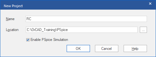
7. Left-click>OK in the New Project dialog to display the Create PSpice Project dialog.
8. Choose empty.opj from the pull-down menu.
This option generates a new project that has a single schematic folder and a single page.
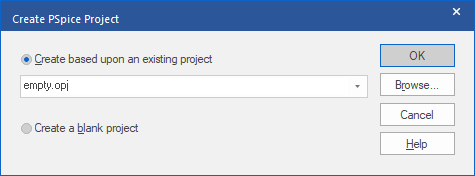
9. Left-click>OK to create the project.
Capture opens with the Project Manager at the left-hand side.
10. Double-click RC.dsn or left-click the plus sign to the left of the design name to expand the display of design contents.
11. Double-click Schematic1 or left-click the plus sign to the left the schematic name to display folder pages.
12. Double-click Page1 to open the drawing window.
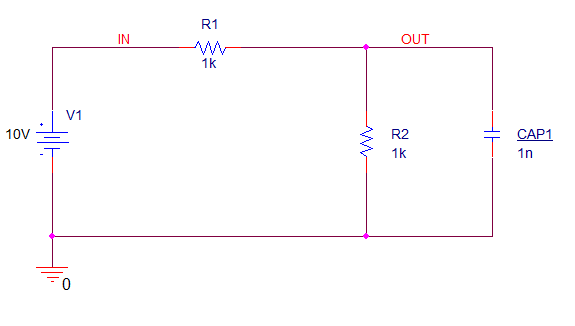
As you complete the remaining steps in this lab, you will be creating the RC circuit shown below.
13. Select Place>Part from the top menu, or press P, or left-click the Place Part icon.
14. Use the Add Library button to add the libraries
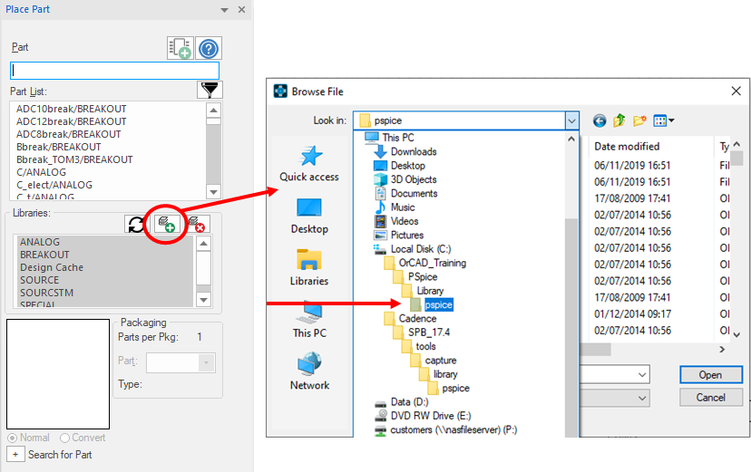
(All of the labs use their own copy of the PSpice libraries provided in the installation located in C:\OrCAD_Training\PSpice\Library\PSpice in addition to the default libraries added from the existing project template which use the libraries from the installation directories)
15. After selecting the C:\OrCAD_Training\PSpice\Library\PSpice directory, left-click the first library entry, 1_shot.olb, scroll down to the end of the library list and use shift+left-click to select the last entry, zetex.olb, selecting all of the libraries, left-click>Open to add the selected libraries.
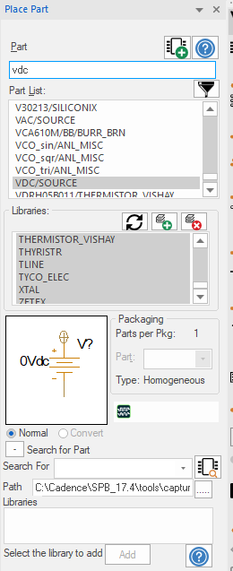
16. Type VDC in the Part edit box for Place Part.
The list scrolls to the VDC entry and the symbol is shown in the preview
17. Double-click on the VDC entry in the Part list, or press Enter.
The VDC symbol is attached to the mouse cursor and the schematic page becomes active.
18. Move the mouse towards the left of the schematic page and left-click to place the source on the page.
(You could use the Esc key, or right-click>End Mode to end the placement command but there are more parts to place in this design)
19. Move the mouse back to the Place Part control and double-click the VDC text in the Part edit box to select and highlight the VDC value, type R in the Part edit box and the selected part entry will change to the R (resistor) part.
20. Double-click on the R entry in the Part list or press Enter to attach a copy of the part to the cursor and move the mouse back to the schematic page.
21. Left-click to place the resistor on the page (R1).
22. Press R to rotate the resistor image attached to the cursor.
23. Left-click to place a second (rotated) resistor (R2).
24. Move the mouse back to the Place Part control again and double-click the R text in the Part edit box to select and highlight the R value, type C in the Part edit box and the selected part entry will change to the C (capacitor) part.
25. Double-click on the C entry or press Enter to attach a copy of the part to your cursor and return to the schematic page.
26. Press R to rotate the capacitor image attached to your cursor.
27. Left-click to place the capacitor on the page (C1 at this point).
28. Press Esc, or right-click>End Mode, to end the placement command.
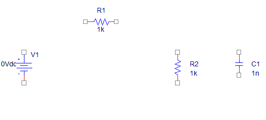
29. Double-click on the C1 text, or left-click on the C1 text and right-click>Edit Properties. Type CAP1 as new the Value and left-click>OK.
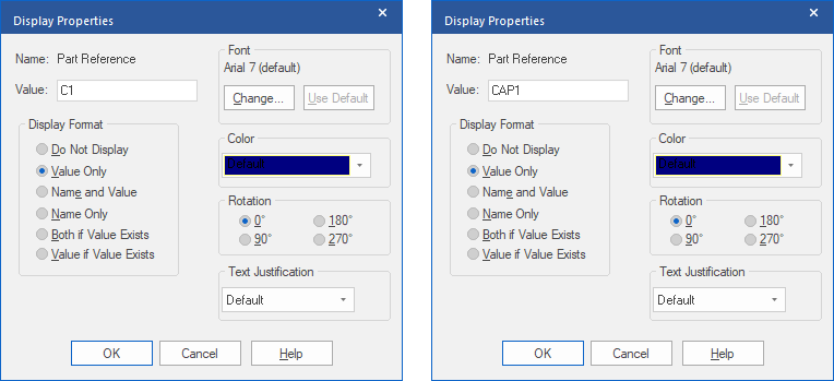
The C1 Reference is changed to CAP1 and the value is underlined to indicate a user assigned value.
30. Select Place>Wire from the top menu, or press W or left-click the Place Wire icon.
31. Wire together the components as shown in the next graphic.
(A completed version of this graphic was also provided earlier in this lab)
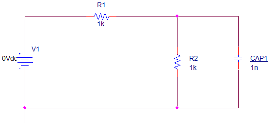
If you make a mistake drawing wires or placing components simply select the item and press the delete key to remove it. You may also left-click the item, then hold down the mouse button, and drag it to the correct location. Wires can be stretched in Capture by selecting the segment and then left-click and drag the end of the segment with the mouse
32. Select Place>Ground from the top menu, or press G, or left-click the Place Ground icon.
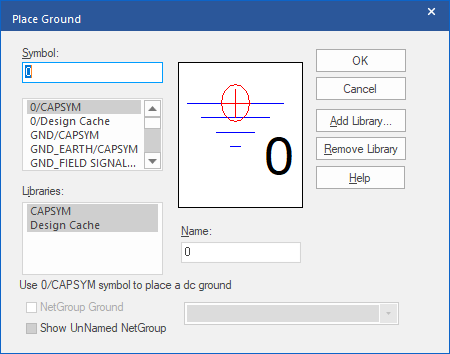
33. Select the 0 (zero) symbol in the part browser, this may already be the selected entry.
34. Left-click>OK to attach a copy of the symbol to your cursor and move the mouse back to the schematic page.
35. Left-click to place the ground symbol to the “stub” shown in the graphics, it may be necessary to draw a wire to make the connection in your schematic.
36. Press Esc, or right-click>End Mode, to end the placement command.
37. Select Place>Net Alias from the top menu, or press N or left-click the Place Net Alias icon.
38. Type IN in the Alias name field.
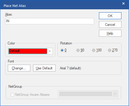
39. Left-click>OK to attach the alias text to the mouse cursor.
40. Left-click on the wire between V1 and R1 to place the Net Alias.
Note that a Net Alias will only “stick” to a Wire (or Bus) and not in “free space” and that the Net Alias text remains on the mouse cursor after the left-click to place it.
41. Either:
a) Left-click to place another “IN” Net Alias between R1 and CAP1; press Esc or right-click>End Mode, to end the Place Net Alias command; then double-click on the IN text between R1 and CAP1 and change the Value to OUT and left-click>OK
or, with the ”IN” still selected, press Control+E and change IN to OUT
or:
b) Press Esc, or right-click>End Mode, to end the Place Net Alias command; then repeat the Place>Net Alias command, this time, set the Value to OUT; place the Net Alias on the wire between R1 and CAP1 and press Esc, or right-click>End Mode, to end the Place Net Alias command
42. In the schematic page, double-click the 0Vdc text shown next to the source.
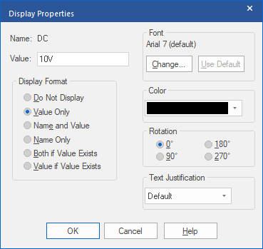
43. Type 10V as the Value for the DC source.
44. Left-click>OK.
45. Select File>Save from the top menu, or left-click the File Save icon.
End of Lab
All content Copyright 2022 Parallel Systems Ltd.