
All content Copyright 2022 Parallel Systems Ltd.
Start PCB Designer from:
Start (Windows Icon) >Cadence PCB 17.4-2019>PCB Editor 17.4
The PCB Editor Canvas opens.
1. Select File>Open from the PCB Editor main menu.
2. If necessary, set the File Type for Board (*.brd)
3. Use the Browse button to navigate to the C:\OrCAD_Training\PCB_Designer_Advanced directory, select the schedule_imp.brd file and left-click on Open
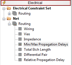
4. Open Constraint Manager and go to Electrical>Net>Routing>Min/Max Propagation Delay.
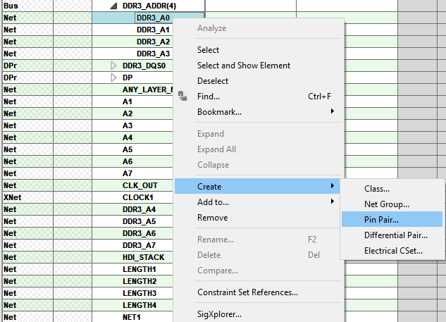
5. Create a pin pair for each of the address signals from U10 to RN1. Select a net and right-click>Create>Pin Pair
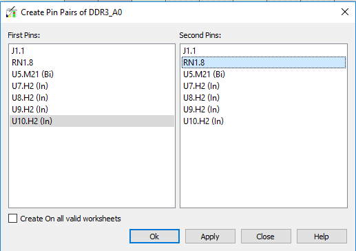
6. Select U10.xx from the left hand list and RN1.x from the right hand list. OK to create the Pin Pair.(OK the message that any Pin Pairs that are created and do not have Constraints attached will be removed when Constraint Manager is closed)
7. Repeat the Create Pin Pair steps for the other three nets of the DDR3_ADDR bus.
8. For each Pin Pair just defined, set a Min value of 10 mm and a Max value of 12 mm
(these need to be assigned to the Pin Pairs, not the Nets or the Bus, otherwise “all” of the Pin Pairs on the Nets will be added…)
9. Locate the DDR3_ADDR bus and right-click>Analyze to “see where you are”, some of the Constraints may be met, or not, these will now be addressed.
(in CM, check Analyze>Analysis Modes for Propagation Delay enabled in Electrical Modes if the nets are not analysed)
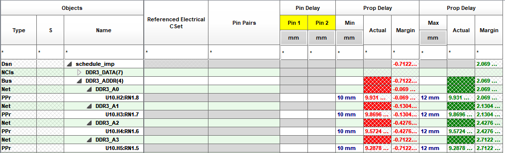
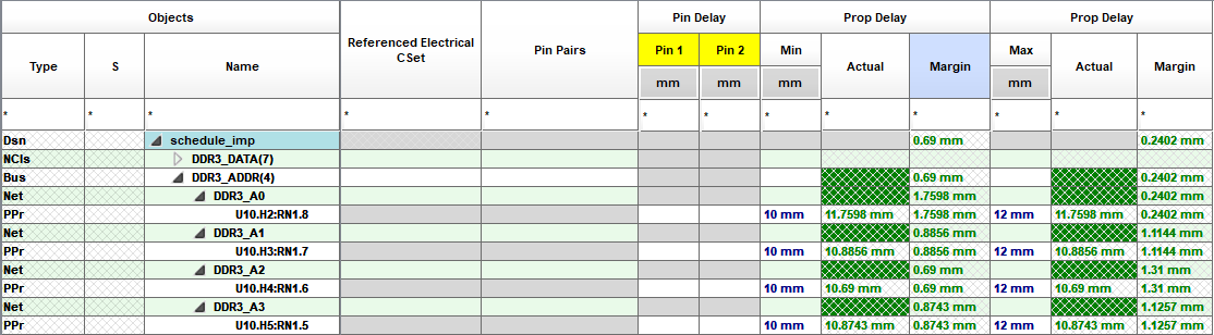
In this case, the routing is less that the Minimum, which gets flagged in red as “not meeting” the Constraint, but this does mean that the routing is less than the Maximum so they get flagged in Green as “meeting”. Both the Min and Max will be “Green” when the Min / Max Constraint is fully met.
10. Go back to the PCB Editor window and locate the connections between U10 and RN1
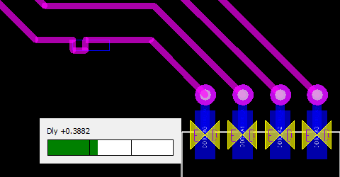
11. Hover over a Connect Line Segment (Cline Seg) in one of the DDR3_ADDR nets and right-click>Delay Tune (if you don’t see this change to Etch Edit Mode) move the mouse to add delay to the routing to match the Constraint. Check the “heads up” display for the current routing vs the Constraint status. Aim to get this “about the middle” but this need not be too critical. Look at Options for delay tune settings.
12. Go back to Constraint Manager and go to Electrical>Net>Routing>Min/Max Propagation Delay and check the Actual vs Constraint to confirm that the routing now meets the set Constraints for the Pin Pairs.
13. Save the Board As schedule_prop.brd

End of Lab
All content Copyright 2022 Parallel Systems Ltd.