
All content Copyright 2022 Parallel Systems Ltd.
Start PCB Editor from:
Start (Windows Icon) >Cadence PCB 17.4-2019>PCB Editor 17.4
The PCB Editor Canvas opens.
1. Select File>Open from the PCB Editor main menu.
2. If necessary, set the File Type for Board (*.brd)
3. Use the Browse button to navigate to the C:\OrCAD_Training\PCB_Designer_Advanced directory, select the schedule_phase_dynamic.brd file and left-click on Open.
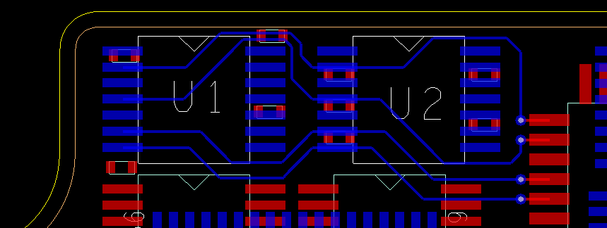
4. Zoom into the top section of the board, you will see some routing between U1, U2 and U20. We want to match the total length of these routes within a minimum and maximum value.
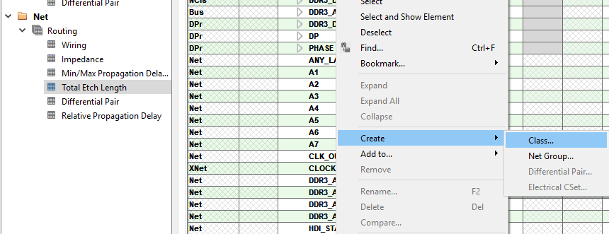
5. Open Constraint Manager and go to Electrical>Net>Routing>Total Etch Length, scroll down through the Nets and locate the LENGTH1 to LENGTH4 Nets, drag select these Nets, right-click in one of the selected Name cells and Create>Class, name the Net Class LENGTH and left-click>OK to create the Net Class.
6. Scroll to the top of the list of nets, the LENGTH Net Class, will have been moved to the top of the list, if necessary, open the LENGTH Net Class to display the members and right-click>Analyze on the LENGTH name.

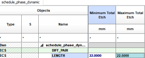
Now the Actual values will be filled in for the current routing, the same value will be shown in the Min and Max groups. In this case, our object is to try to match the lengths within about 0.5 mm of the longest routed member. Your numbers may vary but, as an example, let’s say that LENGTH1 is the longest and has a currently routed length of 22.0943 mm, setting the Constraint Min to 22.0 mm and Max to 22.5 mm will be sufficient in this case.
Once you have values for the Min and Max requirements, you can set the Constraint values and apply the Constraint to the LENGTH class.
7. Open the Electrical Constraint Set>Routing>Total Etch Length and, in the “schedule_phase_dynamic” cell, right-click>Create>Electrical CSet and name the new Constraint Set LENGTH.
8. Left-click on the “black triangle” in the “schedule_phase_dynamic” cell to open the constraint list and set the Min and Max values calculated above.
9. Return to Nets>Routing>Total Etch Length, locate the LENGTH class and select the LENGTH Constraint Set from the drop-down in Referenced Electrical CSet cell. The values from the Constraint Set will be filled in.
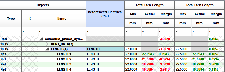
10. If necessary, right-click>Analyze in the LENGTH cell to get the net “actual” and “required” routing lengths checked. The longest net should be fine, since this was used as the reference for your calculation but the other nets may well be outside the required limits.
(Green: actual values meet the Constraint, Red: actual values fail to meet the Constraint) It’s likely that the Min values will be “short”, and Red, the MAX values will all be Green since they are less than the required Max value.
11. Go back to the PCB Editor window, the Constraint Manager window can remain open so that it can be re-visited after the routing is corrected.
12. Zoom in on U1 and U2 and locate one of the traces that does not meet the Total Etch Length requirements, there should be an “E L” DRC for the nets that need correcting. (Check that all the DRC colours are enabled in Display>Color / Visibility if you are not seeing the DRC markers in the design)
13. Using the methods you learned earlier add delay to the clines that require it. The routing will initially have a “tracer” through the route indicating that the Length rule is not being met and the “heads up” display will indicate “red”, negative value means “short”
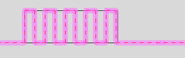
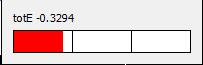
Trace does not meet requirement, “short”
As the Length meets the rule the “tracer” will clear from the routing and the “heads up” display will indicate “green” “meets”
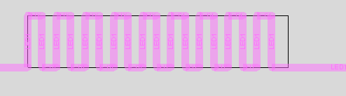
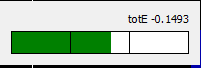
Trace meets requirement
The “tracer” will return again as the added delay increases the Length beyond the required Maximum and the “heads up” display will turn red again.
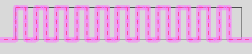
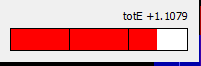
Trace does not meet requirement, “long”
14. Left-click to accept the routing when corrected.
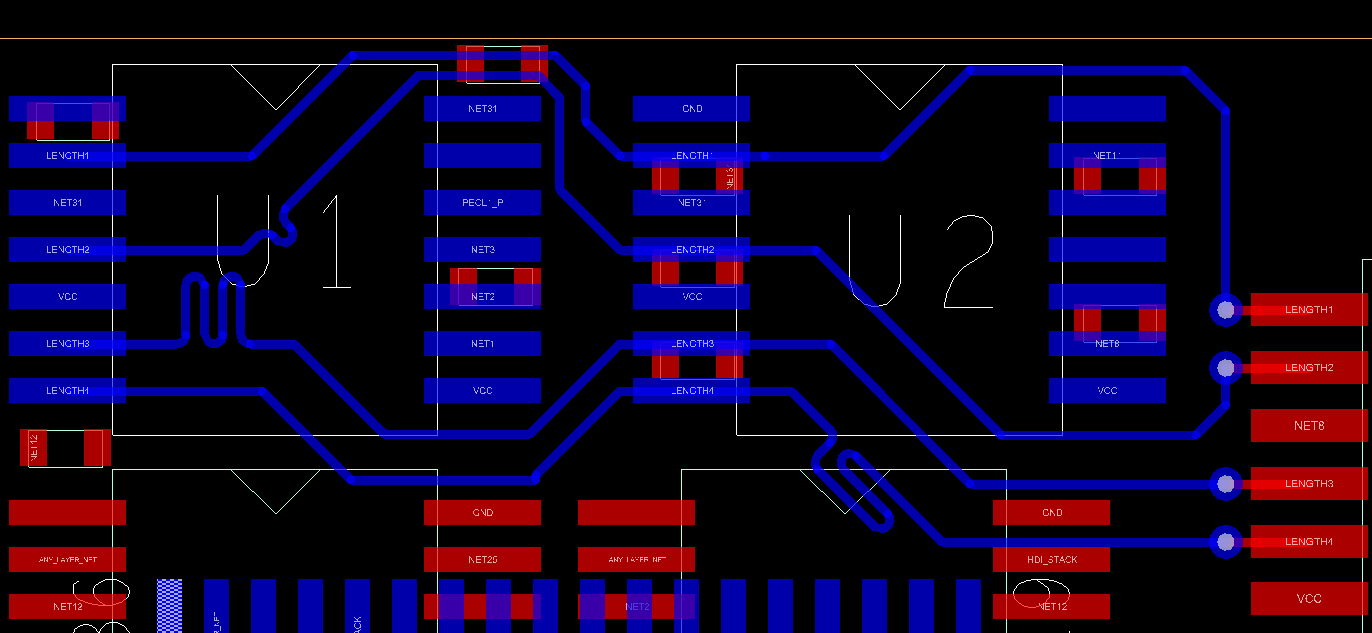
You can add lengths that meet / don’t meet and see what the effect is in the Constraint Manager. You can also change the Delay Tune parameters in the Options tab to see what effect they have. The “gap” for the delay routing comes from the One times the Line to Line Same Net Spacing rule OR Three times the Min Line Width Physical rule in Constraint Manager.
15. Save the board as schedule_complete.brd

End of Lab
All content Copyright 2022 Parallel Systems Ltd.