
All content Copyright 2022 Parallel Systems Ltd.
Start PCB Editor from:
Start (Windows Icon) >Cadence PCB 17.4-2019>PCB Editor 17.4
The PCB Editor Canvas opens.
1. Select File>Open from the PCB Editor main menu.
2. If necessary, set the File Type for Board (*.brd)
3. Use the Browse button to navigate to the C:\OrCAD_Training\PCB_Designer_Advanced directory, select the rigid_flexi_start.brd file and left-click on Open
4. The first step is to ensure the MATERIALPATH is set to the local directory. Go to Setup>User Preferences>Paths>Config and edit the MATERIALPATH to include the directory where the training files are stored. (This includes a material.dat and masklayerssitefile.xml) which are used in this lab.
Note: Remember to set your MATERIALPATH back to your usual location once the training course is complete.
5. Invoke the Cross Section Editor from the Setup>Cross Section or the Cross Section icon.
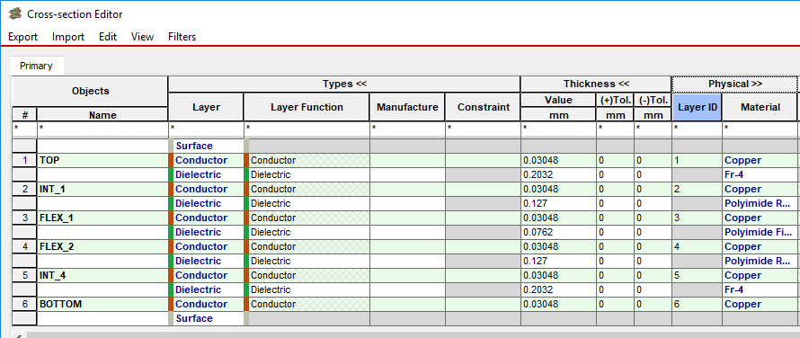
The stackup is currently defined as a 6 layer board
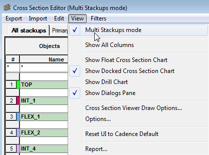
6. Enable “Multi Stackup Mode” from the View>Multi Stackups Mode
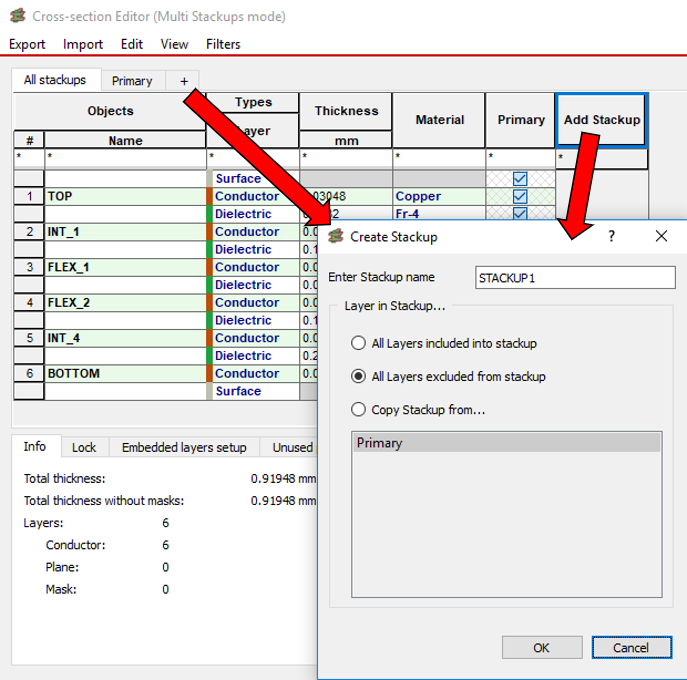
7. Add a new stackup to be targeted as a Flex zone. Click the “+” sign or the “Add Stackup” column header. In the Enter Stackup name field, rename the default stackup name from Stackup1 to Flex1.
Enable the All Layers excluded from stackup option. This will not assign any layers to the FLEX1 stackup from the Primary stackup. Click OK to add the stackup. .
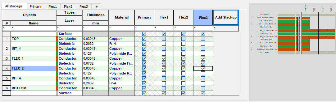
8. Repeat step 7 to add Flex2 and Flex3. Configure all three stackups as shown below. There should be 3 layers enabled (Flex_1, Dielectric and Flex_2).
9. We now want to add some mask layers to the cross section. Select the Layer Top and right click>Add Layers
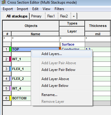
10. In the Add Layers interface enable Above Conductor TOP, left click on the Arrow (>) next to Design-defined Mask Layers and left click Soldermask Top, confirm the layer function (Solder Mask) and the Layer Material which displays the possible mask materials defined in the materials.dat file. Scroll down the list and choose Soldermask Flexible Lpi and click on Add (Do not click on Exit). The Soldermask_Top layer is added to the cross section.
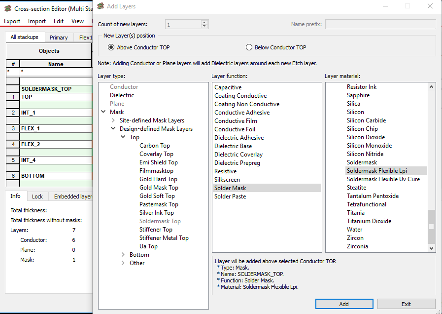
11. With the Add Layer form still open, select the BOTTOM layer cell in the Stackup editor. Notice how the layer name changed in the New Layer Position form.
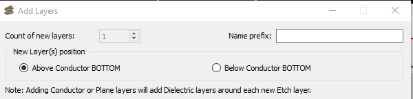
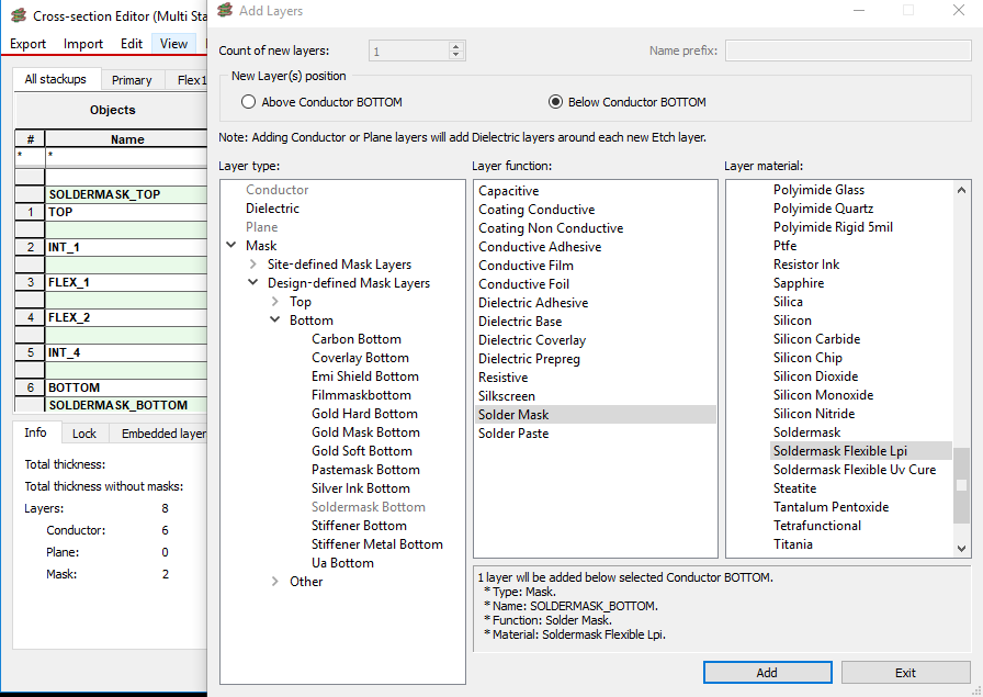
12. Perform the same steps to add Soldermask_Bottom below the Bottom layer. Be sure to select the option Below Conductor BOTTOM.
13. Using the techniques you have learned above, add the following mask layers from the Design and Site defined layers.
Note: Site defined layers are layer materials that you can add and control manually. To create/edit a site file go to Edit>Site File and add any layers you need. This is also controlled by the materialpath variable so store the masklayerssitefile.xml in this location.
COVERLAY_TOP – Dielectric Coverlay – Polyimide – Thickness 0.038mm.
COVERLAY_BOTTOM – Dielectric Coverlay – Polyimide – Thickness 0.038mm.
ADHESIVE_TOP – Dielectric Adhesive – Adhesive Epoxy – Thickness 0.025mm
ADHESIVE_BOTTOM – Dielectric Adhesive – Adhesive Epoxy – Thickness 0.025mm
STIFFNER_TOP – Dielectric Base – Fr-4 – Thickness 0.2032mm
SOFT_GOLD_BOTTOM – Coating Conductive – Gold Soft Bondable – Thickness 0.003556mm
If you have made a mistake in the mask layer order you can adjust this by using the Edit>Mask Layer Order command which allows you to move the layers up and down as required. Ensure your stackup matches the screenshot below.
14. The final step is to configure the stackups with their correct layers. Check / un-check the mask layers for flex1, 2 and 3 to match the screenshot below.
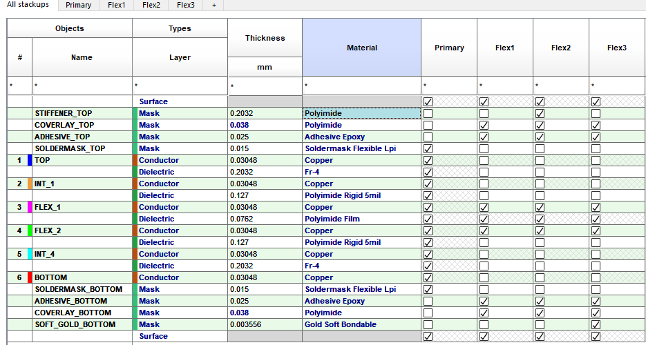
You can select each tab to examine the cross section defined for each stackup group. The info tab at the bottom also displays the thickness for each cross section.
15. Click on Apply to save the stackup. Then click on OK to close the form. Save the board as rigid_flexi_stackup.brd.

End of Lab
All content Copyright 2022 Parallel Systems Ltd.