
All content Copyright 2022 Parallel Systems Ltd.
Start PCB Editor from:
Start (Windows Icon) >Cadence PCB 17.4-2019>PCB Editor 17.4
The PCB Editor Canvas opens.
1. Select File>Open from the PCB Editor main menu.
2. If necessary, set the File Type for Board (*.brd)
3. Use the Browse button to navigate to the C:\OrCAD_Training\PCB_Designer_Advanced directory, select the rigid_flexi_zones.brd file and left-click on Open
4. Just outside the bottom right corner of the board are two components, U7 and J1. Using standard placement techniques (Setup>Application Mode>Placement Edit or Edit>Move) place the two components on the board as shown below. Before you place them in their correct locations experiment placing them in different zones or on the rigid parts of the design to see the differing results. Try mirroring the parts to see the difference in layers used depending on the zone they are placed in which corresponds with the stackup defined in the initial lab. This is known as Dynamic Placement.
Once placed go to Setup>Colors>Geometry and Component folders and notice that additional subclasses have been added corresponding with the layers the placed components are on. Subclasses for Assembly, Place_Bound, Silkscreen, Soldermask and Pastemask have all be added dynamically. 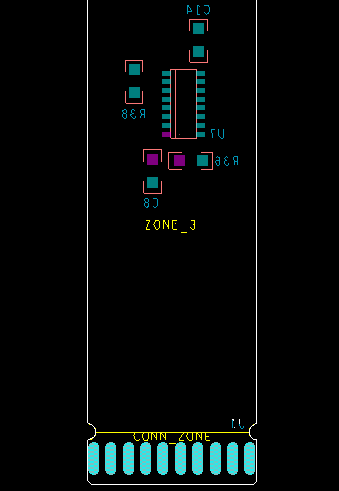
5. Use Display>Show Rats>All, change the application mode to Etch Edit (right click>Application mode>Etch Edit) and route some of the connections in the different zones. Try routing connections that cross multiple zones, add vias using the Working Layers method and see that only the layers that are available based on each stackup are available to route on. You do not need to complete the routing on this lab, it is just an example of the dynamic routing capabilities of PCB Editor and zones.
You do not need to save this board since the next lab will use a pre-routed version to generate Manufacturing data.

End of Lab
All content Copyright 2022 Parallel Systems Ltd.