
All content Copyright 2022 Parallel Systems Ltd.
Start PCB Editor from:
Start (Windows Icon) >Cadence PCB 17.4-2019>PCB Editor 17.4
The PCB Editor Canvas opens.
1. Select File>Open from the PCB Editor main menu.
2. If necessary, set the File Type for Board (*.brd)
3. Use the Browse button to navigate to the C:\OrCAD_Training\PCB_Designer_Advanced directory, select the backdrill_complete.brd file and left-click on Open.
4. Zoom into pin J2B2.B20 using Find By Name in the Find Filter tab.
We want to step through the layers which are backdrilled to review the backdrill clearance keepouts. To make this easier to display these layer specific clearance keepouts we can add Route Keepouts to the Visibility Tab.
5. Choose Setup>Colors then go to the Visibility Pane Tab. The left side of this tab contains visibility pane configurations that are stored in the CVSettings.xml file located in a users %HOME%\pcbenv folder. These settings will be used for all future PCB Editor sessions but if you wish to reset the settings back to default just select the Reset Defaults button.
6. Under the Classes section double click Rte KO (Route Keepout) from the Available Classes or select using the up arrow to move it to the Visible Classes section.
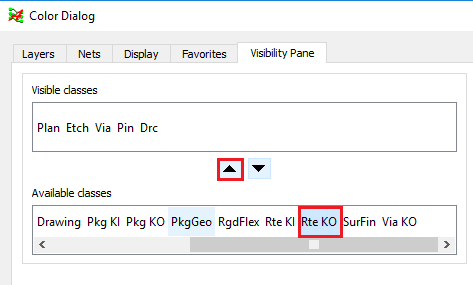
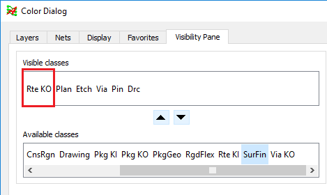
7. Close the Color Dialog and you will now see a new column for Route Keepout on the Visibility Pane.
8. Select Enable Layer Select Mode at the bottom of the Visibility tab to allow quick single click selection to display layers.
9. Select the hyperlink style text (underlined blue text) for Bottom to turn off all other layers and just turn on the BOTTOM subclasses. Notice that the Route Keepout Bottom Subclass is now being displayed automatically when the Bottom side is displayed.
10. Backdrill sites will have a layer specific Route Keepout Shape added to maintain clearance to the Backdrill Hole – based on value entered in the Padstack under BACKDRILL_CLEARANCE Keep Out Geometry.
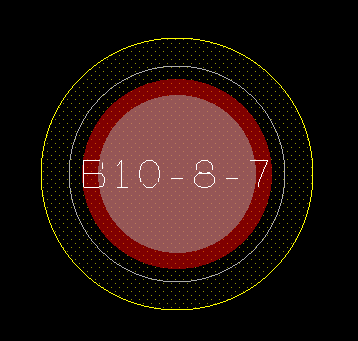
11. Select the hyperlink style text (underlined blue text) for Layer_8 to turn off all other layers and just turn on the LAYER_8 subclasses.
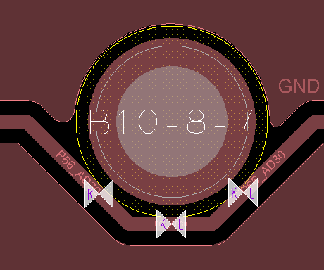
12. The added Route Keepout Shape at the Backdrill site has caused a DRC Error with an existing trace while the Dynamic shape has automatically voided to the keepout.
Note: BACKDRILL_CLEARANCE Keep Out Geometry will be used on all backdrill site locations except on Negative Plane Layers where the BACKDRILL_CLEARANCE Anti Pad Geometry will be used..
13. Notice the Regular Pad above is still displayed even though it is a backdrilled layer. This pad could be suppressed during manufacturing output but it is recommended to enable “Dynamic unused pads suppression” in the design cross section to:
- Avoid a larger than expected clearance based on the pin/via to copper spacing constraints which is greater than the Backdrill Keepout Clearance.
- Prevent an internal pad from being present during manufacturing output if the suppression is not done at the time of output
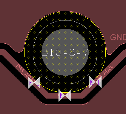
Unused Pad Suppression enabled in the Cross Section.
14. To dynamically suppress the unconnected pads open the Cross Section Editor (Setup>Cross Section) and make the following updates:
- Enable “Unused Pin Suppression“ and “Unused Via Suppression“ in each of the Layer rows under the Physical Column Header, double-click the Physical header to “open” the Physical settings if the Unused Pin / Via Suppression settings aren’t visible.
- Enable “Dynamic unused pads suppression” under the Unused Pads Suppression tab.
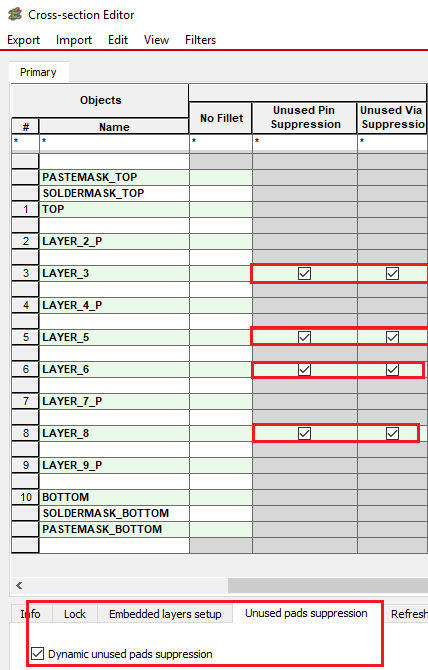
Note: DRC Errors and Dynamic Shapes status may become Out of Date due to suppression settings change.
- Dynamic Shapes may need to be updated to smooth using the Update to Smooth button in the Status Form (Check>Status).
- DRC may need to be updated using the Update DRC button in the Status Form (Check>Status).
15. Save and overwrite the design as backdrill_complete.brd. We will use this design in the next lab.

End of Lab
All content Copyright 2022 Parallel Systems Ltd.