
All content Copyright 2022 Parallel Systems Ltd.
OrCAD PCB Editor Professional has the ability to check for Differential Pair Static Phase tolerance. This is essentially used to ensure that the length or delay of the nets in a differential pair is within a user-defined constraint.
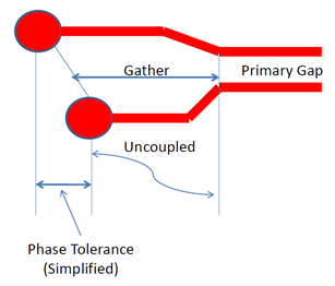
You can set a phase tolerance in length units or time but the length of the two nets in the pair must be matched within that tolerance or a constraint violation is flagged. The phase tolerance is used to accommodate physical issues in a board layout that would prevent two nets in a pair from being routed at exactly the same length. These issues can include placement issues or issues regarding routing blockages in the design.
A simpler definition can be a onetime check from Driver to Receiver comparing lengths of each member. If a Driver cannot be determined, the check is performed across the longest path of the pair.
For a complete application note on Differential Pairs please refer to:-
https://www.parallel-systems.co.uk/wp-content/uploads/2020/02/diffpair_definition.pdf
Firstly a re-cap on the complete setup for a Differential Pair. The first part of this lab will go through creating a differential pair, then a physical and electrical ruleset to apply to the differential pair. We will then route the pair to visualize the ruleset.
There are several methods to create differential pairs from OrCAD Capture to the Auto Setup inside Constraint Manager, to model defined via Signal Explorer. This example is the simplest method from within Constraint Manager.
Start PCB Editor from:
Start (Windows Icon) >Cadence PCB 17.4-2019>PCB Editor 17.4
The PCB Editor Canvas opens.
1. Select File>Open from the PCB Editor main menu.
2. If necessary, set the File Type for Board (*.brd)
3. Use the Browse button to navigate to the C:\OrCAD_Training\PCB_Designer_Advanced directory, select the schedule_pindelay.brd file and left-click on Open
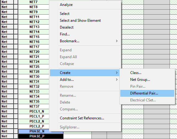
4. Open Constraint Manager>Electrical>Net>Routing>Differential Pair and locate two nets PHASE_N and PHASE_P. Select both netnames and then right-click>Create>Differential Pair
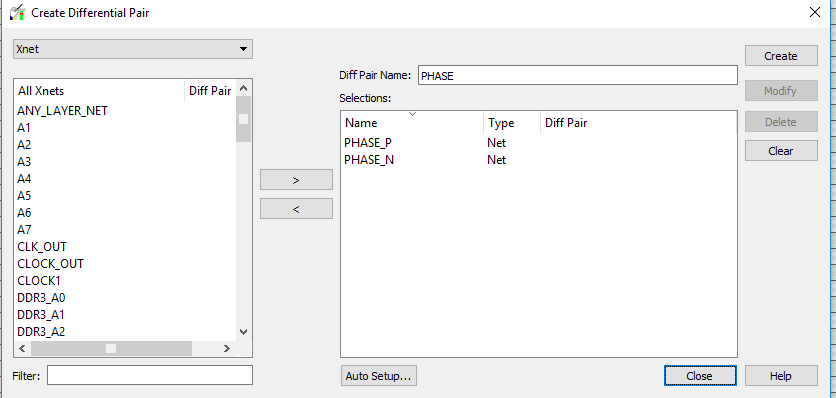
5. Specify a name (if required, the default of PHASE is sufficient), and left-click>Create to define the two connections as a differential pair, left-click>Close.
Note:- Differential Pairs can be defined as an Electrical CSet or a Physical CSet. You can define Min Line Spacing, Primary Gap, Primary Width, Neck Gap, Neck Width, + and – Tolerance as either a Physical or Electrical CSet.
The difference being that if you wish to change the track thickness and spacing as the differential pair changes layers in the PCB to control impedance they should be defined as a Physical CSet.
This is also true if you wish to use Constraint Regions to control a different set of design rules by area e.g. smaller track and gap widths.
For Constraint Regions the differential pairs MUST be defined as a Physical CSet. Uncoupled length and static phase must be defined as an Electrical CSet, so you may find you have both an Electrical CSet and a Physical CSet to control the differential pairs.
If the track thickness and gap remains the same throughout the cross section of the PCB then it is recommended that the differential pair be defined as an Electrical CSet.
You will see the values for Min Line Spacing, Primary Gap, Primary Width, Neck Gap, Neck Width, + and – Tolerance will be inherited from the Physical / Electrical domains depending on how they are defined.
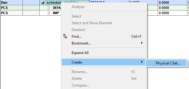
6. In Constraint Manager go to Physical>Constraint Set>All Layers. Select the Dsn name and right-click>Create>Physical CSet, specify a name DiffPair and left-click>OK.
We now need to define values to setup the differential pair. The following two screenshots detail the settings required for a differential pair:-
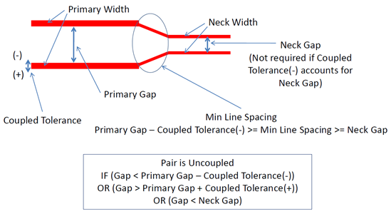
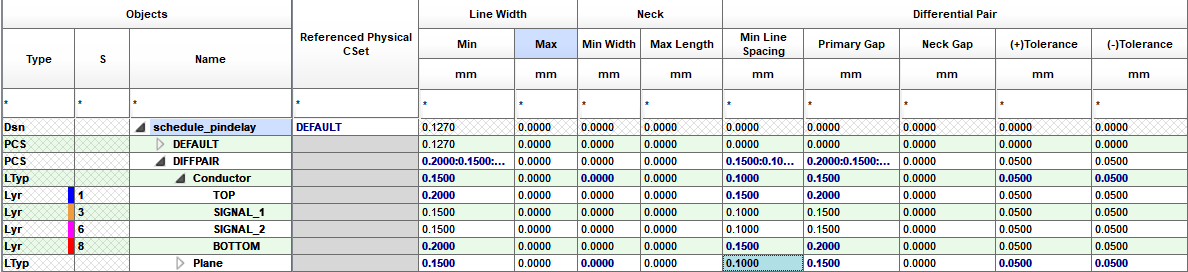
7. Enter the following values for the differential pair:-
a. Min Line Width 0.2mm for outer layers, 0.15mm for inner layers.
b. Primary Gap 0.2mm for outer layers, 0.15mm for inner layers.
c. +/- Tolerance 0.05mm for all layers.
d. Min Line Space 0.15mm for outer layers, 0.1mm for inner layers.
8. Now the Physical CSet has been defined go to Physical>Net>All Layers and apply the Diff_Pair CSet to the differential pair PHASE.
9. The next step is to define the electrical rules for the differential pair. In Constraint Manager, Electrical>Electrical Constraint Set>Routing>Differential Pair and create a new ECSet called Diff_Pair. Enter Gather Control = Ignore; Uncoupled Max Length = 7.5mm. Leave all other cells blank as we are using the Physical CSet to drive these rules and step 12 will discuss static phase.
(If values are entered in the Electrical CSet, they will take precedence over rules set from a Physical CSet.)
10. Apply the Electrical CSet to the PHASE Differential Pair in Electrical>Net>Routing>Differential Pair.
11. Now go to PCB Editor and route the differential pair. Change layers to see the effect of the different physical rules per layer.
12. Open Constraint Manager and go to Electrical>Net>Routing>Differential Pair.
13. Expand the DP entry and specify a Static Phase constraint of 0.127mm for the differential pair DP. If the signals in this differential pair have a length difference larger than 0.127mm it will result in a DRC error.

14. On the board a DRC error will be shown for the longest signal in the differential pair. To fix the DRC error in this example the best course of action is to add a Phase “bump” to add length to the DP_N net, the net without the DRC error. The DRC will inform your of the actual mismatch.
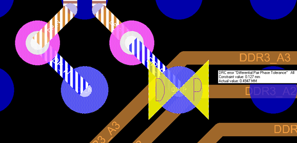
To add phase bumps, you can either use the Route>Delay Tune command but with Single trace mode enabled (right click during the command) then use the heads up display to add the correct amount of delay or the Route>Phase Tune command, where you can specify the size of the bump added in the Options pane before you add the actual bump.
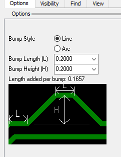
Experiment using both commands if time permits.
Phase tolerance is the choice between matching the length to a certain tolerance and ensuring that the differential pair remains coupled across the complete length. In some instances having the differential pair coupled is more important than matching the length (so uncoupled when you add phase bumps) but the ultimate decision is yours.
15. Save the board as schedule_phase.brd

End of Lab
All content Copyright 2022 Parallel Systems Ltd.