
All content Copyright 2022 Parallel Systems Ltd.
If necessary, start PCB Editor.
1. Select File>Open from the PCB Editor main menu.
2. If necessary, set the File Type for Board (*.brd)
3. Use the Browse button to navigate to the C:\OrCAD_Training\PCB_Designer\project\allegro folder and select the b4route.brd file (saved from Lab 12-2, or use the board from Lab 12-3, if it was only partially routed) and left-click on Open.
4. Select Shape>Global Dynamic Parameters from the main menu.
5. On the Thermal Relief Connects, set the drop-down selection for “Thru Pins” to “Full Contact”
6. Select OK to accept the change.
7. Use File>Save As and change the name to autoroute.brd
8. Select Route>PCB Router>Route Automatic.
(The sequence is slightly different with an OrCAD PCB Designer Standard license: Route>PCB Router>Route Net(s) by Pick from the menu then right-click>Setup in the canvas to get the setup form below.)
The Automatic Router dialog appears. The PCB Editor is now in the background.
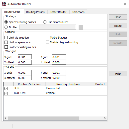
9. Select Router Setup tab, if necessary, select the “Specify Routing Passes” option.
(You may have more available routing layers if you are using a board saved from Lab 12-3)
10. Select the Routing passes tab, change the settings to match the dialog below:
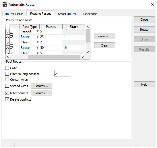
Left-click the check box to enable the Fanout pass
Left-click in the drop-down below “Clean” and select “Route”, the first selection adds the entry, left-click in the drop-down and select “Route” again to add
Left-click in “Passes” for “Route” and set the value to 50, left-click in the “Start” for this row and set the value to 16
Left-click in the drop-down below the added Route entry and select “Clean”, left-click the drop-down again to set the “Clean” and left-click in “Passes” and set the value to 5
Left-click the “Miter corners” and “Delete conflicts” options to enable them
11. Left-click the Route button to start running the autorouter in the background.
(Again this is slightly different with an OrCAD PCB Designer Standard license: left-click>Close on the Automatic Router form, then drag the mouse to “window select” the entire board for “all nets” and auto-routing will start. When completed right-click>Done in the canvas to accept, right-click>Cancel to reject. Step 12 is irrelevant if using an OrCAD PCB Designer Standard license.)
12. When the autorouter completes, the board view will be updated with the routing. Left-click>Close to accept the results, or left-click>Undo to reject them.
13. Restore the Thermal Relief setting for the through pins:
Shape>Global Dynamic Parameters, Thermal Relief Connects tab, set the “Thru Pins” to Diagonal or Orthogonal as required. Use OK to close the Global Dynamic Shapes dialog and accept the change.
14. In the PCB Editor, select File>Save As from the top menu.
A browser form appears.
15. In the File Name field, enter:
autorouted.brd
16. Left-click>Save.
The autorouted.brd file is saved to disk.
End of Lab
All content Copyright 2022 Parallel Systems Ltd.