
Padstacks are used for mounting components, “where the component Pin meets the copper”, mounting holes for the board, and Vias used to route between the layers of the board.
Types of Padstacks
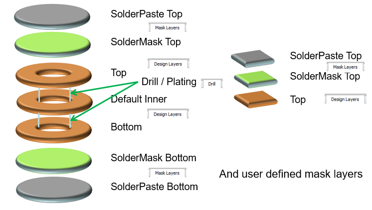
Padstacks are defined for “through hole”, the component Pin goes though the board, or a mounting hole is required to mount the board in an enclosure, and a hole is drilled, or a slot routed, as part of the manufacturing process and defined as part of the Padstack.
Or, Padstacks are defined for “surface mounted”, the component Pin is only attached to an outer layer, traditionally the Top, or Bottom, layer of the rigid structure of the board but possibly within the rigid structure (embedded component) or on a flexible section now.
Padstack Editor, Design layers
Within the Padstack Editor Design Layers: the Begin Layer is closest to the component, connects the Pin, and typically defines the Top Layer in the board; the Default Inner defines any inner layers that the Pin, or Via, is connected to, there can be 2 to 198 Inner Layers in PCB Editor; the End Layer is furthest from the component, connects the Pin, and typically defines the Bottom Layer in the board. For just an edge connector, the End Layer may be the only layer defined for connection on the Bottom Layer only. For all other surface mount pads, these are typically designed on the Top side because when used in a board design bottom is the default “mirror” layer of top.
For a Padstack Layer, only the Regular Pad definition is required. Definitions of Thermal Relief, reduction of the connection to ease soldering of Pins connected to copper areas, and Anti Pad, clearance in copper areas, are not required for copper areas defined as positive dynamic shapes (as used in this course).
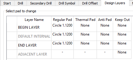
If the pin requires an irregularly shaped pad, a Shape Symbol can be defined in PCB Editor and attached to the definition of the Padstack.
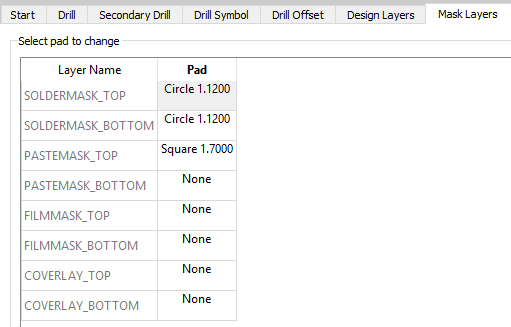
The Soldermask defines a “hole” in a “resist” layer to allow Pins to be connected, this could be defined as “null” for Vias but then they cannot be used as testpoints.
The Pastemask defines a “hole” in a mask to allow solderpaste to be applied to the board, typically required for any “reflow” processing, this could also have a “null” definition if solderpaste is not required.
On the Drill tab, the drill is typically defined with the “finished size” and the fabricator will “oversize” the drill and then plate back to the required “finished size”. For some applications, the hole size is the critical parameter, in which case, the drill tool size is specified, this will define the size of the drill used and then plating will reduce the actual hole that is seen, typically to allow the plating to be “distorted” to make a connection.
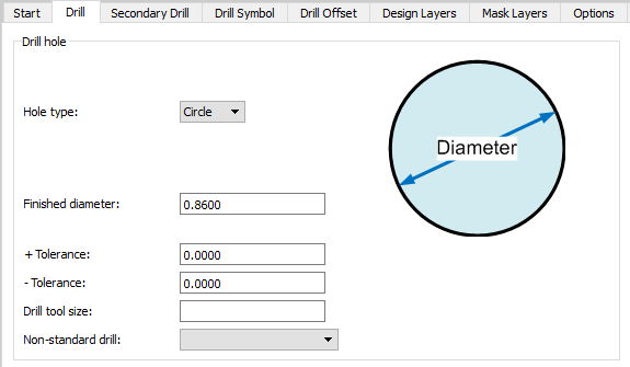
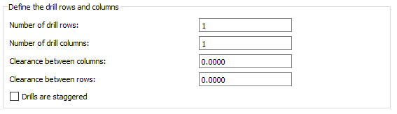
If the Padstack is to be used by a Pin that provides thermal connections to other layers, multiple drills, up to a maximum of 100, can be defined on the Drill tab, then only one Pin will be required in the Package Symbol.
Padstacks need to be defined before Package Symbols, component footprints, can be defined.
The Padstack Editor uses IPC-2581 definitions related to Padstacks for Types and Shapes.
Saving the Padstack definition will result in a “pad” file.
All content Copyright 2022 Parallel Systems Ltd.