
Some essential information about using PCB Editor
Picking a license
When OrCAD PCB Editor starts, there will be a prompt for a license, Cadence Product Choices, pick a license to start running the product.
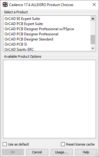 Note that, the first time that OrCAD PCB Editor starts, the license manager is polled for available license features and a list of available licenses is written to a “license cache”, a text file local to the machine. If the mix of available licenses changes, use the “Reset license cache” to refresh the locally stored list.
If the “Use as Default” is selected, that will be the only license checked for, even if other licenses are available.
Starting a new design
When starting a new design, File>New, the choices for design file type are: Board, physical layout; Board (Wizard), run through a wizard to create an initial board and set of rules; Package Symbol, footprint; Package Symbol (Wizard), run through a wizard to create a Package Symbol, footprint; Mechanical Symbol, a symbol that won’t be connected; Format Symbol, typically a “drawing blank”; Shape Symbol, a Shape that will be used in a Padstack; Flash Symbol, part of a Padstack required for negative artwork or a pastemask “chequerboard” opening (not covered in this course)
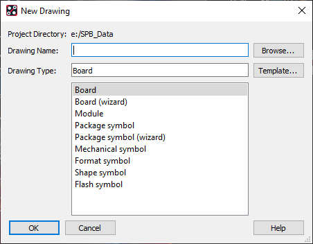
A board file will have a file extension of “brd” when saved, the symbols will have a “dra” file created when saved and the appropriate symbol file, binary equivalent for PCB Editor, created when the symbol is successfully saved: “psm” for Package Symbol, “bsm” for a Mechanical Symbol; “ssm” for a Shape Symbol; “osm” for a Format Symbol and “fsm” for a Flash Symbol.
A new design, of any type, will have the Drawing Origin (0,0) located at the lower left corner of the PCB Editor “world”, this can be changed from Setup>Design Parameters, Design tab, or from Setup>Change Drawing Origin and then selecting a new Drawing Origin with a left-click in the design window, or using the right-click>Snap Pick To>(an object in the design window)
Window layout
PCB Editor starts with the Menu and Toolbars at the top.

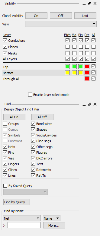
Visibility and Find to the left
The Design Workflow, Options and Command Window to the right
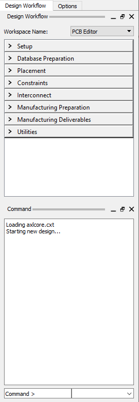
The Options tab activated
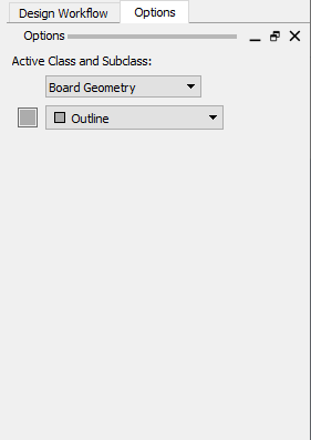
The Options, Find, Visibility, Command and World View can be re-arranged by left-clicking and dragging the grey bar next to the name. Blue guides are displayed to indicate what the arrangement will be if the mouse is released. These can also be placed on a second monitor away from the main canvas window.
Design parameters
Design Parameters, Design tab sets the design units and accuracy.
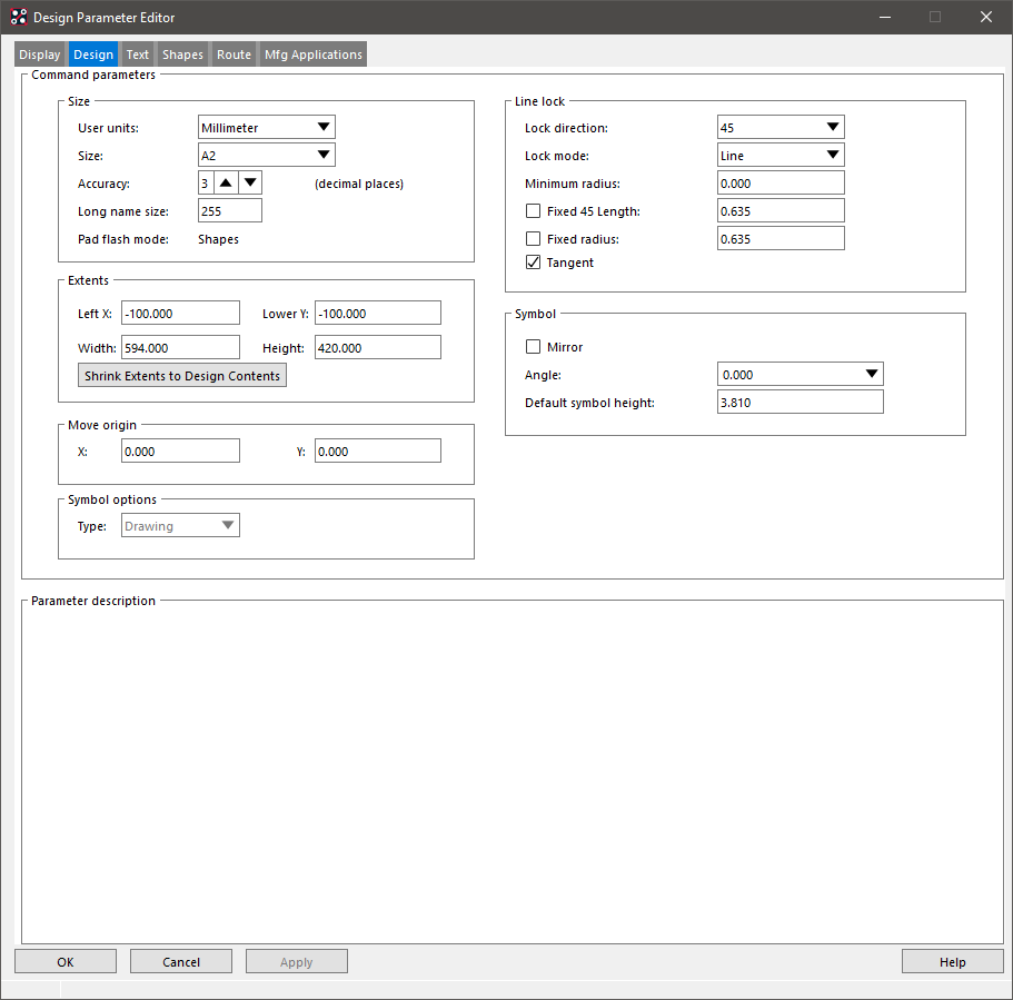
Note that the design units are actively maintained so take care when changing the Units and Accuracy and check any messages about a loss of accuracy since the resolution of the board design will be changed. Typically, the units and accuracy are determined at the start of the design and never changed.
Find and Filtering selections
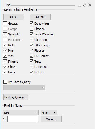
When the mouse is clicked to make a selection, the list of object types in Find is searched down the left column and then down the right-column and the first object type encountered will be selected. Note that “Text” is a long way down the list. The Command Window will indicate if there was any enabled object type that could be selected.
Colours and Visibility
Setup>Colors from the menu gets to “Colours and Visibility” which controls what is displayed and which colours are used for that display. There are buttons to control Global (All) Visibility. Colours in the Layers tab are organised by Classes and Subclasses, see later topic.
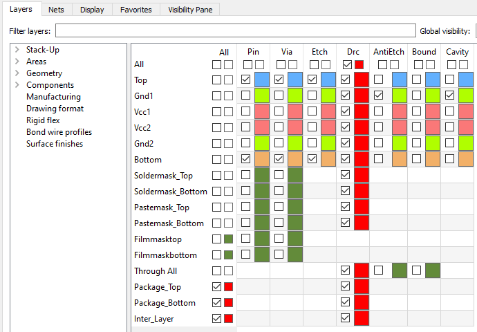
The Visibility checkboxes are in the left column and the colour assignments are in the right-column. Colours can be selected from the colour palette at the bottom of the form, select a colour with a left-click and then left-click in the colour tile for the cell, row, column, or “All” to assign the colour.

15 patterns can be assigned in addition to the colour assignment to distinguish objects.
Preferences
Preferences “fine tune” the behaviour of the product.
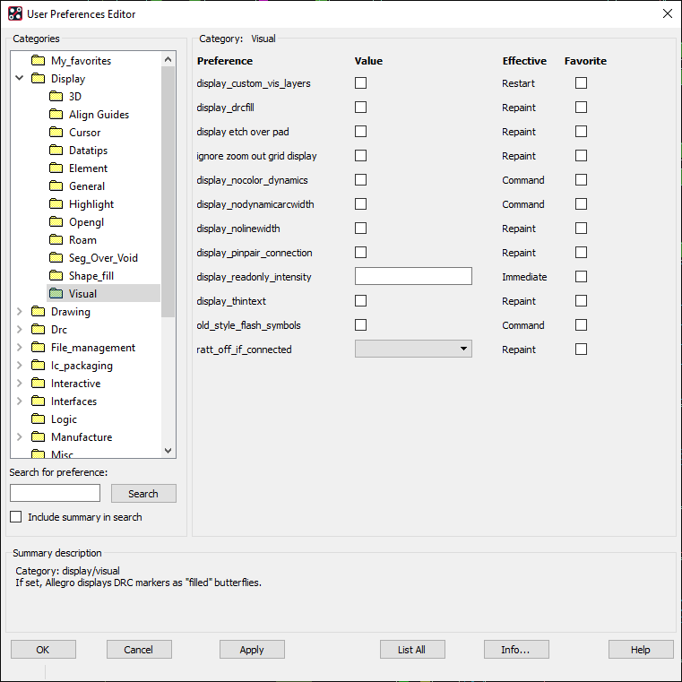
The only preferences considered during the course are the library locations for “padpath” and “psmpath”
Pan and Zoom
Pan and Zoom are controlled with the mouse wheel, roll the wheel to zoom in and out, hold click and drag the wheel to pan. The keyboard arrow keys can also be used for panning. Note that the “wheel-click” is often assigned to the Windows “Flip” action which may not work with PCB Editor, check the mouse settings and assign another mouse button to “middle-click” if required.
Classes and Subclasses
Objects in the PCB Editor database are organised by Classes and Subclasses, this allows for objects to be selectively displayed in the canvas, or grouped for output (artwork). The Classes are fixed but up to a total of 200 subclasses may be created for each Class. There are a number of predefined Subclasses but, whilst the intended use is implied from the names, except for areas, PCB Editor does not strictly enforce what the Subclasses are used for. Areas: Keepins, Keepouts and Boundaries are used in design rule checking. Keepins restrict the overall area of the design and Keepouts are used to restrict the design within the Keepins. Boundaries, like the Place Bounds for Package Symbols for example, are used to define the extents of components and the DRC checks these against the Package Keepin.
All content Copyright 2022 Parallel Systems Ltd.