
All content Copyright 2022 Parallel Systems Ltd.
1. Start PCB Editor from:
Start (Windows Icon) >Cadence PCB 17.4-2019>PCB Editor 17.4
The Cadence Product Choices form may appear
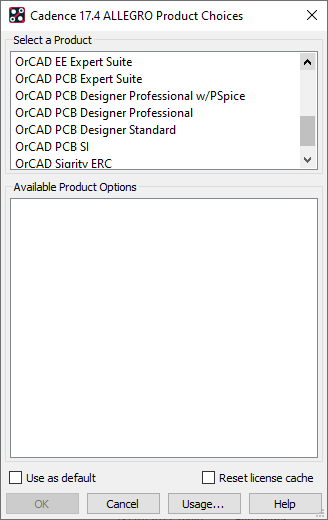
2. Select any OrCAD PCB Designer license, then left-click>OK.
3. Select File>New from the top menu.
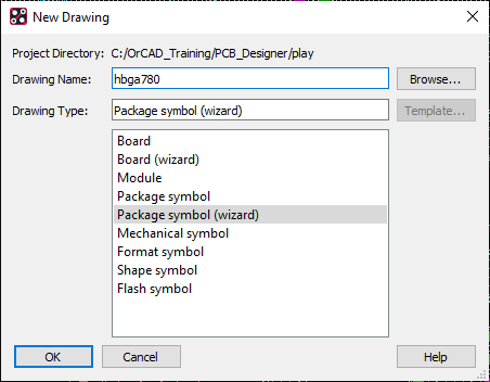
The New Drawing form appears.
(Left-click>No if prompted to save any open files)
4. Use the Browse button to browse to the C:\OrCAD_Training\PCB_Designer\play directory
5. Type the following name in the Drawing Name field:
hbga780
6. Select Package symbol (wizard) from the scrolling list of drawing types, as shown below:
7. Left-click>OK to close the New Drawing form.
The Package Symbol Wizard form is displayed. This form is used to specify the type of package symbol to be created.
8. Choose PGA/BGA as the type of Package Symbol Wizard to be used.
9. Left-click Next> to use the PGA/BGA wizard and continue to the next form.
The Template form is displayed.
10. Choose Default Cadence supplied template.
11. Left-click>Load Template to load the default template.
12. Left-click Next> to continue to the next form.
The General Parameters form is displayed.
13. Set the values of Units to Millimeter and Accuracy to 2 for the fields Units used to enter dimensions in this wizard and Units used to create package symbol, if these values are not currently set.
14. Set the Reference Designator Prefix to U* if this value is not currently set.
15. Left-click Next> to continue to the next form.
The Pin / Ball Grid Array Pin Layout form is displayed.
16. Set the Vertical and Horizontal pin counts to 28 and check the Full Matrix option.
17. Left-click Next> to continue to the Pin Ordering option, select Number Right Letter Down and Jedec Standard for the naming.
18. Left-click Next> and set the Lead Pitch to 1.00 for Vertical and Horizontal and the Package dimensions, Width and Length, to 33.00
19. Left-click Next> and use the “…” buttons to browse for the c050 padstack designed earlier, left-click on the padstack entry and OK the padstack selection The same padstack will be used for all of the pads.
20. Left-click Next> to get to the next stage of the Wizard.
21. Left-click Center of Body Symbol as the location of the symbol origin (if this option is not currently selected).
22. Left-click Create a compiled symbol for whether or not the Package Symbol Wizard should generate a compiled symbol (if this option is not currently selected).
23. Left-click Next> to continue to the next form.
The Summary form is displayed.
24. After verifying that the files hbga780.dra and hbga780.psm will be created, select Finish to complete the Package Symbol Wizard and create the hbga780 symbol.
At this point you can make any changes that you require. If you do make changes, be sure to save the drawing and create the symbol.
The package that has been generated has 784 pins, rather than the required 780 pins. This package is not going to be used in any of the subsequent labs but, if you wish, you can use hover the mouse over the four corner pins and right-click>Delete from the pop-up menu to delete them.
Keep PCB Editor open for the next Lab.
End of Lab
All content Copyright 2022 Parallel Systems Ltd.