
All content Copyright 2022 Parallel Systems Ltd.
1. Start PCB Editor if you don’t already have the software running.
2. Select File>New from the top menu.
3. In the Drawing Name field, type:
outline
4. Choose Mechanical Symbol from the drop-down list of drawing types:
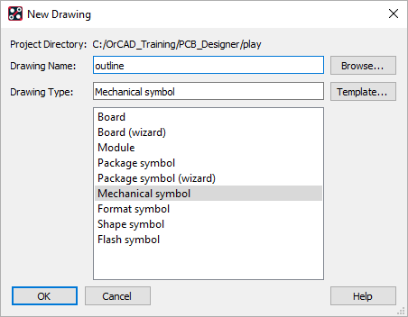
5. Check that “play” is still the Project Directory and left-click>OK to start the new symbol in PCB Editor.
6. Left-click>OK on the “Create a new design” form
7. Move the mouse into the canvas background and right-click>Quick Utilities>Design Parameters from the pop-up menu.
8. Left-click the Design tab.
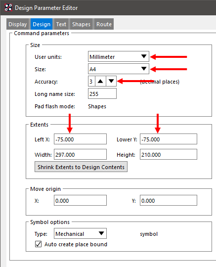
9. Check / Set the Design tab parameters to match the values in the following figure.
10. Left-click the Display folder tab in the Design Parameters form.
11. Select the Setup Grids browser button:

12. In the Non-Etch section at the top of the form, make the following spacing changes:
a. Double-click in the Spacing: x field and enter: 0.5
b. Double-click in the Spacing: y field and enter: 0.5
13. Left-click>OK at the bottom of the Define Grid form.
14. Left-click>OK to close the Design Parameter Editor form.
15. Choose Shape>Polygon from the top menu.
16. Check / Set Options Active Class and Subclass:
Board Geometry / Design Outline
17. Left-click in the PCB Editor Command Window and type in the following entries,
pressing Enter after each entry:
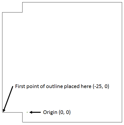
x -25 0
ix 20
iy -10
ix 100
iy 120
ix -100
iy -10
ix -20
(be sure to type lower case letters for the commands)
18. Move the mouse to the canvas and right-click>Done to end Shape / Polygon.
19. Select Layout>Pins from the top menu or select the Add Pin icon 
20. Move the mouse to Options, left-click the Browse (….) button in the Padstack field,
select:
Twistslot
21. Left-click>OK on the Select a padstack form.
PCB Editor Command Window states:
Using ‘TWISTSLOT pad’.
22. Left-click in the PCB Editor Command Window and type the following command to place the twistslot pad at 0, 0:
x 0 0
23. Then press Enter.
24. Move the mouse back to Options and browse for another padstack, use Hole110 for the remaining mounting hole padstacks:
25. Left-click in the PCB Editor Command Window and type the following commands to place the remaining mounting holes:
x 0 103
x 90 -5
Press Enter after each command.
26. Move the mouse to the canvas background and right-click>Done from the pop-up menu.
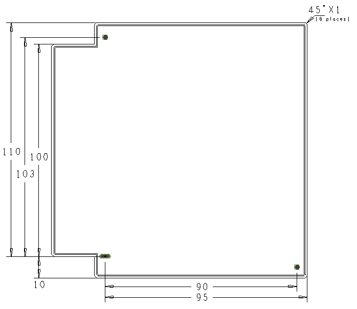
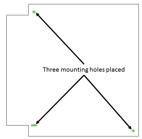
Three tooling holes are now placed within the board outline. Your outline should look like the next figure.
27. Zoom to display the lower-left corner of the outline, then select Setup>Application Mode>Shape Edit from the top menu.
Options will change to show shape editing options.
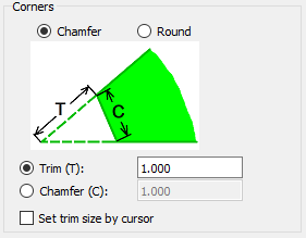
28. Check that Vertex Commands, Click is set to Chamfer / Round, in the Corners section check that Chamfer is selected and change the Trim (T) value to 1.0, as shown in the following illustration:
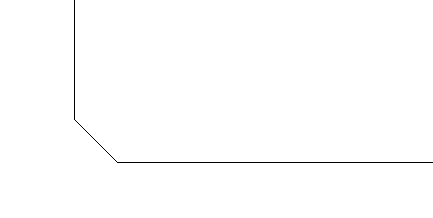
29. Move the mouse to the lower left corner and hover over the corner intersection of the outline, the cursor will change to a four-pointed cross, left-click at this point and the corner will be trimmed back by the specified Trim amount.
30. Repeat the chamfer for the remaining “outside” corners.
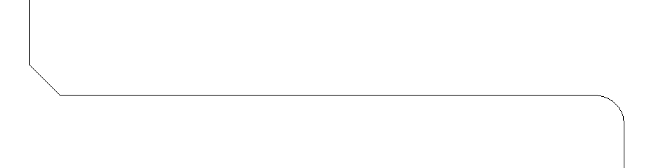
31. Change the Corners option to Round, choose the Radius (R) and set the value to 1.0, then “round” the two “inside” corners.
32. Select Setup>Application Mode>General Edit from the top menu.
33. Select Dimension>Dimension Environment from the top menu.
PCB Editor enters the Dimension editing mode in which all commands are activated from the right-clicking in the canvas.
34. Right-click in the canvas to bring up the Dimensioning menu, choose Parameters.
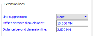
35. Left-click on the Lines tab, complete the Extension Lines box as shown in the figure.
36. Left-click>OK to accept the new value and close the Drafting Parameters form.
37. Pan to view the bottom half of the board, then right-click>Linear Dimension
Options will change to BOARD GEOMETRY and DIMENSION.
(If required, use Display>Color / Visibility to assign a colour to the Board Geometry / Dimension subclass)
38. Zoom in to get the lower section of the board in view, left-click on the Twistslot to specify the start of the dimension
The PCB Editor Command Window prompts for a second point for the dimension value.
39. Zoom out to get the board in view and zoom in again to the right hand edge and left-click on the round mounting hole.
40. Zoom out again to view the board and note that dimension extension lines are following the mouse to allow X, or Y, dimension to be added, move the mouse to the lower edge of the outline to get a X Dimension and left-click to set X as the required dimension, the dimension value will appear on the cursor, make a final left-click to set the X dimension in the required location with respect to the lower edge of the board.

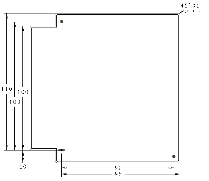
41. Following the same procedure used to add dimensions, place dimensions, as shown in the next screenshot:
(Using the Twistslot as the dimension start will reference dimensions to the datum)
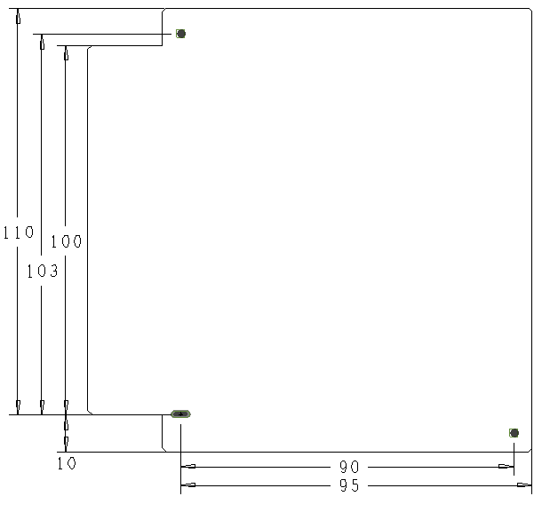
Note that the screenshot does not show the board “fully dimensioned”, this is not important for the purposes of the Lab.
42. When you have finished adding the Linear Dimensions, right-click>Next from the pop-up menu.
43. Zoom in to the chamfer at the upper right corner.
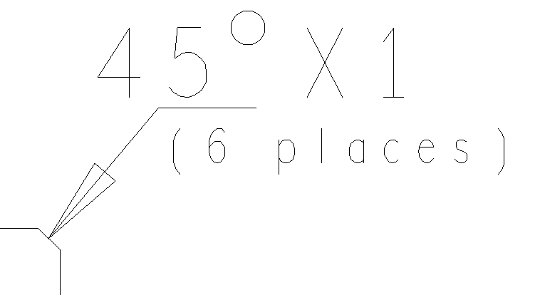
44. Right-click>Chamfer Leader from the pop-up menu.
(If, by some chance, you selected Done at the last command, use Dimension>Dimension Environment to re-enter the Dimension Environment, then right-click to get the pop up menu for Chamfer leader)
45. Left-click on the 45-degree chamfer line.
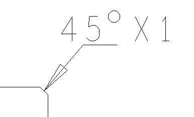
The dimension text is attached to your cursor. (See example in the next screenshot)
46. Move the mouse to “pull” the cursor up and to the right, then left-click to create a leader line. The leader line is the line between the dimension text and the 45-degree chamfer. (Use the left-click to add some more leader line sections, as required). Be sure to pull the text away from corners on the leader line, then right-click>Next to place the “chamfer dimension text” and remain in the Dimension Environment.
47. (Optional) Right-click>Next and right-click>Radial Leader, move to one of the “internal” corners and left-click to start the leader and pull the dimension away from the corner, this will simply display R1 for a 1mm radius.
48. Right-click>Done to place the dimension and exit the Dimension Environment.
49. Select Add>Text from the main menu to place a text note specifying the number of chamfers on the board. In Options, set the text parameters to match these:
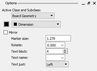
Look in the PCB Editor Command Window prompts as to which action to perform.
50. Left-click to specify the text position and then type “(6 places)” as the text as shown in the next figure and right-click>Done from the pop-up menu.
51. Select View>Zoom Fit from the top menu to view the entire board.
52. Select Edit>Z-Copy Shape from the top menu.
53. Move the mouse to Options, set the Copy To: Class / Subclass to PACKAGE KEEPIN and ALL.
In the Shape Options group:
Offset: 1.5
left-click Contract
54. Move the mouse to the canvas and left-click on the design outline.
A package keepin is drawn 1.5 (mm) inside the boundary of the board outline.
55. Move the mouse back to Options, set the Active Class and Subclass to ROUTE KEEPIN and ALL. In the Shape Options group:
Offset: 1.0
(and make sure the Contract option is still enabled)
56. Left-click and select the design outline again.
A route keepin is drawn 1.0 (mm) inside the boundary of the board outline. Your board outline should resemble the following figure.
57. Move the mouse to a blank area of the canvas and right-click>Done to end the Z-Copy command.
58. Select Setup>Areas>Package Keepout from the top menu.
59. Use left-clicks to define the corners of a polygon shape near the centre of the board (anywhere within the outline will do).
When the polygon is closed, it is automatically filled with a pattern, indicating a static shape. Remember, these are being added as an exercise, they will be deleted later in this lab.
60. Right-click>Done from the pop-up menu.
61. Zoom into the area around the mounting hole at the bottom left of the board.
62. Select Setup>Areas>Route Keepout from the top menu.
63. Use left-clicks to draw a rectangle around the mounting hole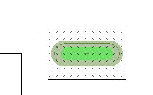
64. Right-click>Done from the pop-up menu.
65. Select Edit>Delete from the top menu.
66. Check / Set the Find Filter for Shapes enabled, then left-click twice on both the Package and Route Keepout shapes you just created. One left-click selects the Shape, the second left-click confirms the Delete.
(Zoom in and out as needed)
Check that the Package Keepin and Route Keepin have not been accidentally deleted.
67. Right-click>Done from the pop-up menu.
68. Select Setup>Areas>Via Keepout from the top menu.
The PCB Editor Command Window prompts you to enter a shape outline.
69. In Options, set the Segment Type option to Line Orthogonal.
This will add only horizontal and vertical line segments.
70. In the PCB Editor Command Window, type each of the following sets of values, pressing Enter after each command:
x -25 5
iy 90
ix 12.5
iy -90
71. Move the mouse to the canvas background and right-click>Done from the pop-up menu. The polygon fills and closes automatically.
The completed outline is shown in the figure.
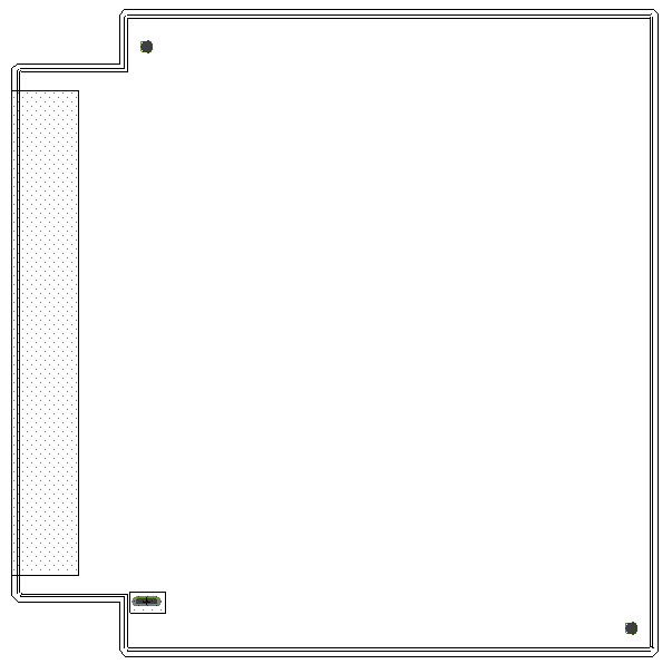
(Dimensions not shown for clarity)
72. Choose File>Save from the top menu.
The system saves an outline.dra file.
The DRA is used if the graphics for this symbol ever need to be edited.
Saving the symbol also executes the Create Symbol process to create a the binary equivalent outline.bsm, which is used in the design process during the building of the board design file in the next section.
The DRA and BSM files should always be stored together.
End of Lab
All content Copyright 2022 Parallel Systems Ltd.