
All content Copyright 2022 Parallel Systems Ltd.
(Start PCB Editor if it is not running)
1. Select File>New from the top menu.
2. Select No to not save the changes just made, if prompted.
The New Drawing dialog box appears.
3. Type the following name in the Drawing Name field:
master
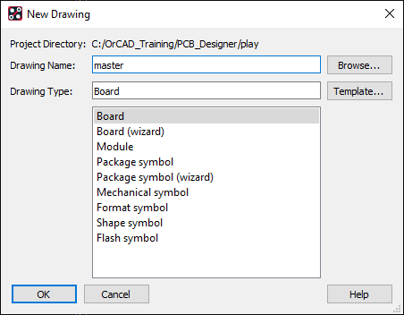
(Check that the Board file is being created in the C:\OrCAD_Training\PCB_Designer\play as the Project directory, use the Browse… button to set this and the “master” file name)
4. Left-click>OK to close the New Drawing dialog box.
5. Left-click>OK on the “Create a new design” form
6. Select Setup>Design Parameters from the top menu.
7. Select the Design tab.
8. Change the settings to match those in the next figure.
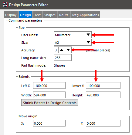
9. Left-click>OK to close the Design Parameters Editor form.
10. Select Place>Mechanical Symbols from the top menu.
11. Check the box to the left of the OUTLINE symbol entry, as shown in the next figure.
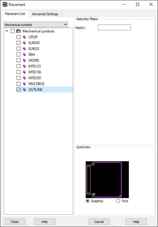
12. Left-click>Hide in the Placement form.
13. In the PCB Editor Command window, type:
x 0 0
14. Move the mouse to the canvas background and Right-click>Done from the pop-up menu.
15. Select Export>Reports from the top menu.
16. In the Reports dialog box, double-click Symbol Library Path Report, making it a Selected Report, and left-click>Generate Reports
A report opens, listing the play directory as the location of where the symbol outline.bsm was found to place on this board.
17. Close the Symbol Library Path Report and the Reports form and zoom out to view the entire design, including the dimensions and text.
18. Left-click the Colour icon. Under the Geometry folder, toggle Dimension off.
19. Left-click>OK to close the Colour Dialog form.
The dimension text disappears, but the board outline remains visible.
20. Choose Display>Zoom>World and then Place>Drawing Symbols from the top menu.
21. Left-click the Advanced Settings tab and enable the Autohide option.
This will automatically hide the Placement form while you are placing a symbol.
22. Left-click the Placement List tab to get back to the list of Format Symbols
23. Check the box for the A3SIZE symbol in the list, as shown:
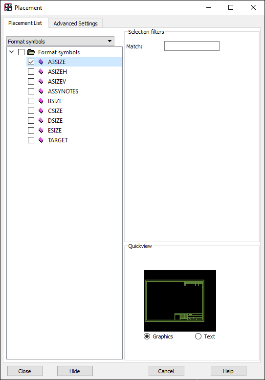
24. Move the mouse to the canvas and left-click to place the drawing format towards the lower left of the “world”. Use the zoom functions as needed. The board should be surrounded by the drawing format outline, but leave some space to the right of the board outline, as shown in the next figure.
25. Move the mouse back to the Placement dialog box, enable the check box next to the name for the ASSYNOTES symbol entry.
26. Left-click to place the notes (on the right side of the board outline, within the format borders), as shown in the next figure.
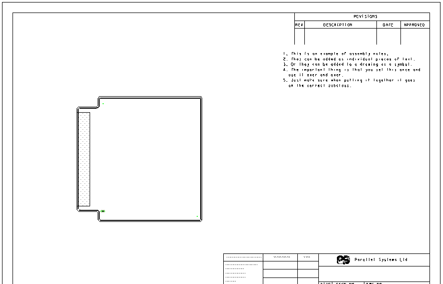
27. Select Package symbols from the pull-down menu in the Placement form.
28. Set the “Match” field to “din*” and press the Tab key, scroll through the list of library symbols and enable the check box next to the symbol DIN64.
29. At the PCB Editor Command Window enter:
x -18 10.5
And press the Enter key to set the location
30. Right-click>Done from the pop-up menu.
The connector is placed.
31. Use File>Save from the top menu, or the “Save” icon, to save the file at this point.
32. Zoom in to the lower left corner of the connector area. Since this master design file is simply a mechanical template with no logical (schematic) database, the edge connector has the reference designator (J*) set in the library part.
33. Select Display>Zoom>Fit from the top menu to see the entire board.
34. Select Place>Components Manually to get back into the placement mode.
35. Left-click the Advanced Settings tab and check the Autohide option is still set.
36. Left-click the Placement List tab.
37. Select Package symbols from the pull-down menu.
38. Set the “Match” field to “connex*” and press the Tab key and enable the check box next to the symbol CONNEX_112659.
39. At the PCB Editor command line, enter the following coordinates:
x 86.5 8.5
And press the Enter key, then select CONNEX_112659 from the Package Symbols list again and enter the following coordinates:
x 86.5 27.5
Again press the Enter key.
(Both connectors are placed on the right edge of the board.)
40. Right-click>Done from the pop-up menu. (Or Close in Place, Manually form)
41. In the PCB Editor Command Window, enter:
replay colours
And press the Enter key.
42. If necessary, select Display>Zoom>Fit from the top menu to zoom into the entire board.
43. Use File>Save again to save the file, OK to overwrite.
44. Select Setup>Cross-section from the top menu.
Notice that TOP and BOTTOM layers are already defined by default as conductor layers.
45. Move the mouse to the right-hand edge of the cross-section dialog and “click and drag” to enlarge the cross-section form.
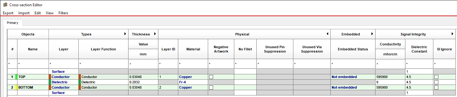
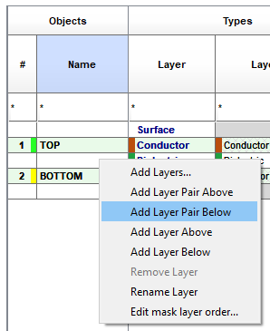
46. Move the mouse to the cell between the layer numbers, 1 and 2, on the left hand side and right-click>Add Layer Pair Below
47. Right-click>Add Layer Pair Below three more times again, don’t worry about which order the default layer names are listed as, this will make a total of 6 conductor layers.
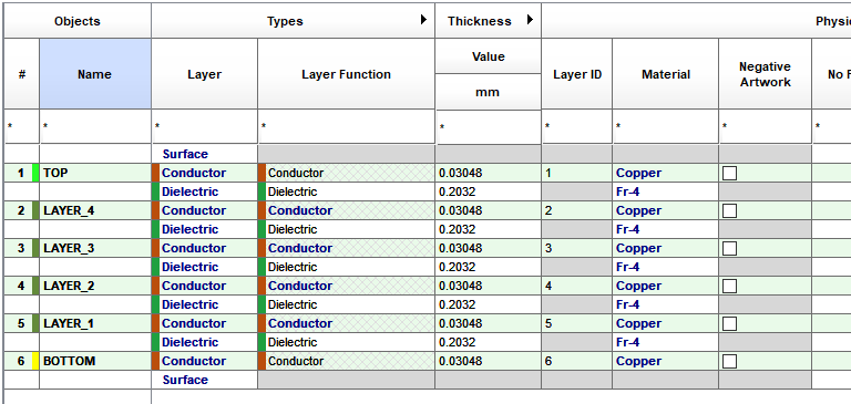
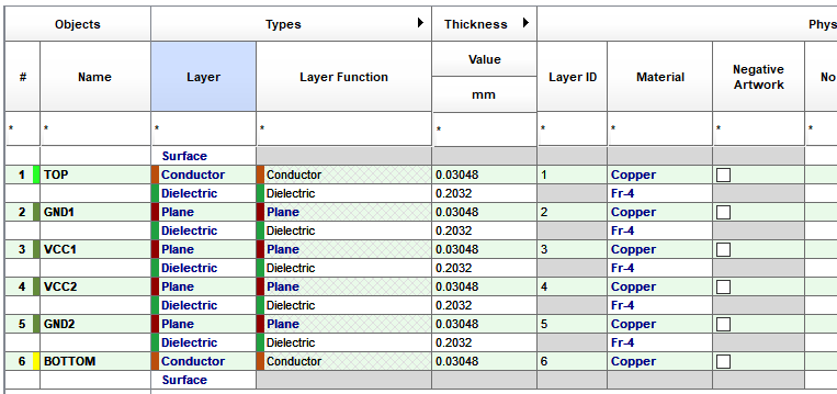
48. Now change the name of the added conductor layers to GND1, VCC1, VCC2, GND2 and change the Types>Layer (and Layer Function) from Conductor to Plane as shown in the next screen shot.
49. Now change the Physical>Material settings for this design. Note that there are a very limited number of materials available for the course material, a lot fewer than the default installation provides. Change the Copper to 0.5 Oz Copper, the “signal” dielectrics to De-156 Sig and the “core” dielectric to De-156 Core as shown in the next screen shot.
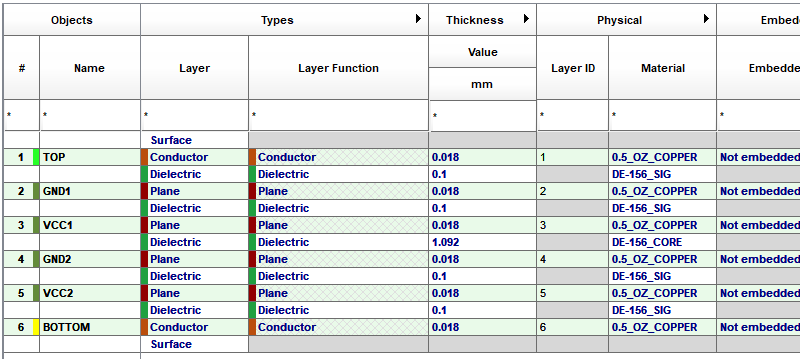
These settings will conveniently make a thickness of 1.6mm in total.
50. Double-click in the “Signal Integrity” header to expand the parameters.
51. Scroll the cross section across to get the Signal Integrity parameters in view and set the Width to 0.15mm, the Diff Coupling to Edge and the Diff Spacing to 0.25mm, this results in “pretty much” 50 Ohm as the trace Impedance and 100 Ohm as the Differential Impedance.
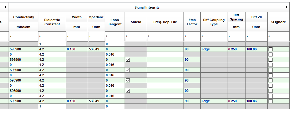
This isn’t an essential step for this design but does illustrate the use of different materials and the impedance calculator in the PCB Editor cross section.
52. Left-click>OK to close the Layout Cross Section form.
53. Select Check>Design Status from the top menu.
54. Set the Dynamic Fill mode to Disabled.
55. Left-click>OK to close the Status form.
56. Select File>Save As from the top menu.
57. Navigate to the working directory which will be used for the rest of the labs.
This will be ../project
(Up one directory level from the “play” directory and then down one directory level into the “project” directory)
58. Check / Set the Change Directory box.
59. Left-click>Save to save the master.brd file in the correct directory.
The master.brd file is saved to disk.
60. Select File>Exit from the top menu to exit the PCB Editor software. You have completed the library development section of this course.

End of Lab
All content Copyright 2022 Parallel Systems Ltd.