
All content Copyright 2022 Parallel Systems Ltd.
1. If you don’t already have the PCB Editor tool running, start PCB Editor.
2. Select File>Open and open the constraints.brd design file you saved previously if it is not currently open.
3. Select Setup>Constraints from the PCB Editor main menu.
The Constraint Manager opens, select the Spacing domain at the left hand side.
4. Select the All Layers in the Spacing Constraint Set folder.
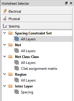
5. In the Default row, change all values to 0.15, as follows, left-click in the Line To to select it and drag the mouse to the Min BB Via Gap cell to the right. Note that entire row highlights and the Min BB Via Gap cell is “open for editing”, type the required value, 0.15 in this case
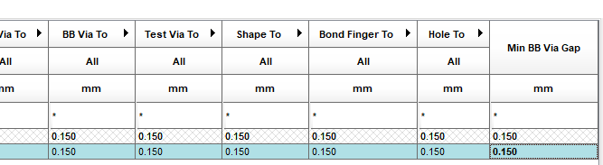
The entire row values will change after a press of the Enter, key.
(You may see an initial entry of *** for the value, setting a value of 0.15 will override all of the values)
6. Left-click the Default cell under Objects / Name.
7. Select Objects>Create>Spacing CSet from the Constraint Manager menu.
(or right-click>Create>Spacing CSet in the Default cell)
8. In the Create Spacing CSet form, enter Clocks for the name and left-click>OK
9. Drag select the cells for the Clocks values and enter 0.2 and press Enter, to change all values to 0.2.
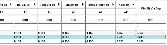
10. Create two more Spacing CSets, Power with all values set to 0.4 and Controlled with all values set to 0.25
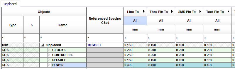
11. Select All Layers under the Net folder.
12. Left-click the “triangle” to the left of the Net Class names to expand the Net Class to see the member names.
13. Select the Referenced Spacing CSet cell in the SYNC row and select Clocks from the pull-down menu.
14. Repeat this to apply the Power Spacing CSet to the POWER Net Class.
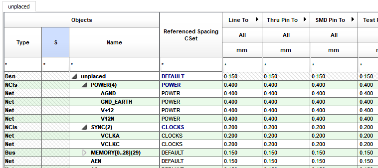
15. Save the design and continue by switching back to the PCB Editor window and using File>Save from the top menu.
16. Left-click>Yes to confirm the overwrite.
The constraints.brd file is once more saved to disk.
End of Lab
All content Copyright 2022 Parallel Systems Ltd.