
All content Copyright 2022 Parallel Systems Ltd.
1. Start PCB Editor and open the constraints.brd file in your working directory if it is not already the open design.
2. Select Edit>Object Properties from the top menu.
3. If necessary, activate Find
4. In the Find By Name section of Find, left-click the scroll button to set the field description box to Comp (or Pin).
5. Left-click in the text entry field, and enter:
j1
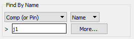
Then press the Tab key, the Edit Property and the Show Properties forms appear. Notice that the J1 connector has no properties attached to it.
6. In the Edit Property form, left-click the Hard_Location and Fixed properties from the list on the left (Available Properties)
These properties then move to the right.
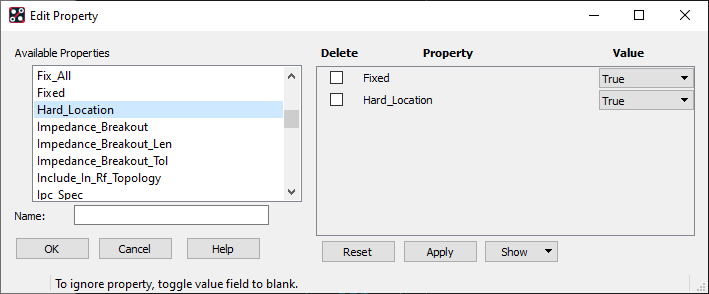
The properties will be True when added.
7. Left-click>Apply.
In the Show Properties window, the properties HARD_LOCATION and FIXED are added to component J1.
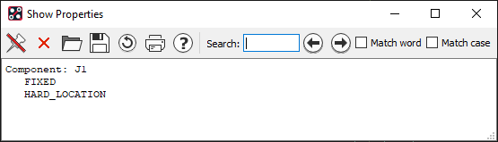
8. Left-click>OK to close the Edit Property form, the Show Properties will also close, then right-click>Done to end Edit>Object Properties command.
9. Select the Fix icon 
10. In the Find Filter, select the All off button, then turn on only Symbols.
11. Left-click on the two Connex connectors on the right side of the board, then right-click>Done to exit the Fix command.
12. Select Edit>Object Properties from the top menu.
13. In the Find By Name section of the Find Filter, scroll to set the field description box to Comp (or Pin), if this is not already set.
14. Left-click>More.
The Find by Name/Property form appears.
15. Set the Name filter to d* and press the Tab key to filter the list, left-click the All-> button to transfer the items on the left to Selected Objects on the right.
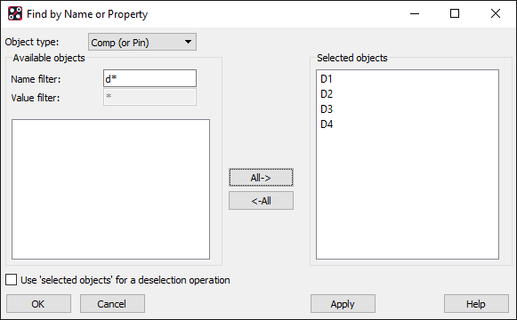
16. Left-click>Apply in the Find By Name/Property form and the Edit Property form opens.
17. In the Edit Property form, select Room from the list of Available Properties in the scroll list on the right.
18. In the blank Value field next to the Room property, enter the room name:
LED
(The ROOM value needs to be Upper Case)
19. Left-click>Apply.
In the Show Properties window, the ROOM property is added to all four components.
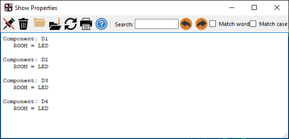
20. Left-click>OK to close the Edit Property form.
21. Left-click>OK to close the Find By Name/Property form.
22. In the Find By Name section of the Find Filter, left-click the drop-down and select Net from the list.
23. Left-click in the blank field under Net, and enter:
vcc
When you press the Tab key, the Edit Property and the Show Properties forms appear.
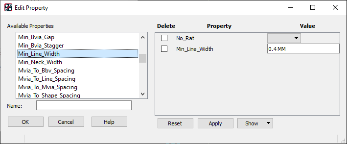
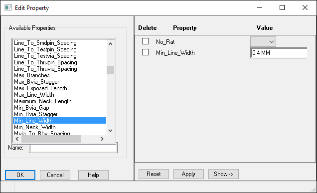
24. Scroll the list in the Edit Property form and left-click on Min_Line_Width.
This property now appears in the right side of the table.
25. In the blank field next to Min_Line_Width property, enter the value of the line width:
0.4 (Units are not required, design units assumed) and press the Tab key.
26. Left-click>Apply.
In the Show Properties window, the Min_Line_Width property is added to the net VCC.
27. Left-click on the Min_Neck_Width to add this property and assign a value of 0.2.
28. Follow the same steps to attach the Min_Line_Width and Min_Neck_Width properties to the net GND, and set the values to 0.4 and 0.2 respectively.
29. Left-click>OK to close the Edit Property form.
30. Move the mouse to the canvas and right-click>Done to end the Edit>Object Properties command.
31. Select Edit>Object Properties from the top menu.
32. In the Find by Name section of the Find Filter, left-click in the blank field under Net, and enter:
*
(asterisk character, shift+8). Press the Tab key, and the Edit Property form displays a list of any properties that have been attached to the nets in the current board file.
The Show Properties window displays all of the nets in the design, and the properties attached to each net.
33. In the Show Properties window, use the “disk” icon  to save the file.
A browser form appears.
34. Enter the following name to save the file:
netprops
35. Left-click>Save in the browser form.
The file netprops.txt is written to the current working directory. This file contains the same information as the Show Properties window, and can be used to check property assignments for the design.
36. Left-click the “cross” icon  in the Show Properties form.
37. Left-click>OK to close the Edit Property form.
38. Select Check>Properties from the top menu.
The Show Property form appears. It contains a scrollable list of properties.
39. Left-click the Room property from the list of Available Properties.
40. Left-click the Show Val button.
The Show window displays a list of functions and components with the ROOM property attached.
(The ROOM property was assigned to D1, D2, D3 and D4 with the value of LED earlier, all other assignments were made in the schematic/net list)
41. Left-click the “cross” in the Show window.
42. Left-click>OK in the Show Property form.
43. Select Edit>Object Properties from the top menu.
44. In the Find By Name section of the Find Filter, left-click the scroll button to set the field description box to Comp (or Pin).
45. Left-click in the blank field under Comp (or Pin), and enter:
j1
When you hit the Tab key, the Edit Property dialog box appears and the Show Properties window displays all of the properties attached to J1.
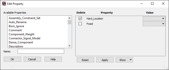
46. Enable the box on the left side of the property named HARD_LOCATION, as shown, then left-click>Apply.
The property disappears from the Show Properties window. These steps can be used whenever you need to delete a property from an element.
47. Left-click>OK to close the Edit Property form.
48. Right-click>Done to exit the Edit>Object Properties command.
49. Select File>Save from the top menu.
A Save window appears, prompting you to decide whether you want to overwrite the existing constraints.brd file.
50. Left-click>Yes.
The constraints.brd file is saved to disk.
End of Lab
All content Copyright 2022 Parallel Systems Ltd.