
All content Copyright 2022 Parallel Systems Ltd.
1. Start PCB Editor and open the placed.brd file if it is not the current design.
2. Select Display>Blank Rats>All to remove the display of ratsnest lines.
3. Select Display>Show Rats>Components.
4. Left-click on a component.
Ratsnest lines appear for all signals that exist on the component you picked. The appearance of the ratsnests is cumulative as you select more components.
5. Select Display>Blank Rats>All again from the top menu.
The Unrats All and Rats All icons also turn ratsnest lines off and on.

6. Select Display>Show Rats>Nets.
7. Move the mouse to the Find filter.
8. In the Find By Name section, select Net from the drop-down list, make sure the next field is set to Name, and enter aen (not case sensitive) in the > field, as shown in the figure:
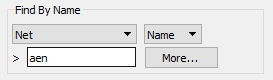
Then press the Tab key. The AEN rat is displayed and the window will zoom around the ratsnest. You could have also left-clicked on a pin if you knew the location of the net.
9. Right-click>Done.
10. Select Display>Blank Rats>All from the top menu.
End of Lab
All content Copyright 2022 Parallel Systems Ltd.