
All content Copyright 2022 Parallel Systems Ltd.
1. Start PCB Editor and open the placed.brd, if the board is not already open.
2. Select Display>Blank Rats>All to turn off all the ratsnest lines.
3. Select Setup>Colors from the top menu or use the toolbar icon.
4. Left-click the Layers tab, left-click the Off button for Global Visibility.
5. Select the Stack Up entry. Set a colour for Pin/Via/Etch for the GND1 and GND2 subclasses and set a colour for Pin/Via/Etch for the VCC1 and VCC2 subclasses. (Green and Purple have already been assigned to the Nets for these layers so, possibly, avoid using those)
6. Go to the Geometry entry and turn Design Outline on (And change colour?)
7. Left-click>OK to close the Color / Visibility form.
8. Select Outline>Z-Copy from the top menu.
9. Left-click on the Options tab, change the Class to ETCH, Subclass to VCC1
10. Change the Size to Contract and the Offset to 1.0 if required.
11. Left-click to enable Create dynamic shape if it is not already set.
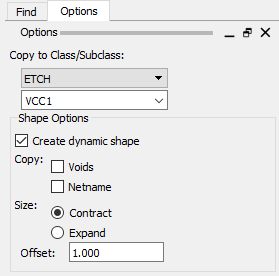
12. Left-click on the Design (Board) Outline in the canvas.
The shape is created on the ETCH / VCC1 subclass. The shape outline, matches exactly, contracted by the specified amount. Right-click>Done in the canvas background to end the Z-Copy command.
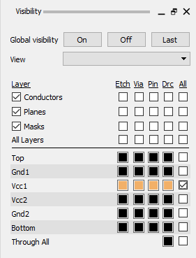
13. Left-click on the Visibility tab to enable it and left-click the “All” check box for the VCC1 layer to see that layer. This will show the created shape “filled in”.
14. Go to Shape>Select Shape or Isolation / Cavity from the menu and left-click the shape just created in the canvas. With the mouse hovered over the selected shape, right-click>Copy to Layers… In the “Shape Copy to Layers” form, expand the entry for Etch, check the boxes for GND1, VCC2, and GND2 layers, set the “Create Dynamic Shape” option and left-click>Copy.
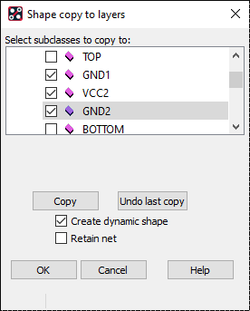
(A total of 4 shapes will now exist in the design)
15. Left-click>OK to close the “Shape copy to layers” form.
16. With the Shape still selected in the canvas, go to Options and left-click the “…” button to the right of “Assign Net Name: Dummy Net” option to browse for Nets.
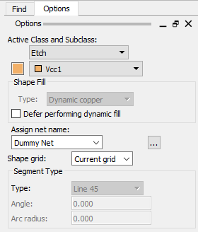
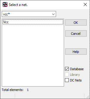
17. Type VCC in the “Select a Net” form. Left-click the Vcc entry and left-click>OK, or double-click the Vcc entry, to set the assigned Net.
18. Right-click>Next in the Background canvas.
19. Go to Visibility and uncheck “All” for VCC1 and check “All” for GND1.
20. Left-click the visible shape in the canvas.
21. Go to Options and use the “…” button to browse the Nets, for this shape select the GND Net from the list and either, left-click the Gnd entry and left-click>OK, or double-click the Gnd entry, to set the assigned Net.
22. Repeat the steps to move to the Next shape, enable the visibility of the Layer and assign the Net Name for the Shapes on the VCC2 and GND2 layers.
Right-click>Done once this has been completed.
23. Select Shape>Global Dynamic Parameters from the top menu.
24. Select the Shape Fill tab, in Dynamic Fill, left-click on Smooth.
25. Left-click>Update to Smooth.
The PCB Editor command window will display a message stating that the GND1, GND2, VCC1 and VCC2 plane shapes are being updated. This will also connect the thermal relief connects with artwork quality voids and thermal reliefs on the layers. These will be visible on the displayed GND1 layer.
26. Left-click the Void Controls tab and check / change Artwork Format to RS274X.
27. Left-click>OK to accept the changes.
28. Go to Visibility and set GND1 as the visible layer
29. Select Shape>Delete Unconnected Copper from the top menu
30. Left-click Options, make sure the Process Layer drop-down is set to GND1.
The unconnected copper areas will highlight in the canvas, look in the World View, if enabled, PCB Editor will automatically zoom in to those areas during the following steps.
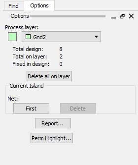
31. Left-click>First in Current Island of Options
The canvas will be zoomed around the first isolated island it finds.
32. Left-click>Delete in Current Island of Options
This removes the first island and creates a void boundary, the canvas then zooms into the second isolated island.
33. Left-click>Delete again in Options and notice that the island count changes from seven to six.
34. In Options, change Process layer to GND2 and delete (all on layer) the islands on the GND2 layer
35. Repeat the processing for the VCC1 and VCC2 layers.
36. Move the mouse to the canvas and right-click>Done to exit the delete unconnected copper command.
37. Select Display>Zoom>Fit to see your entire design, or use the toolbar icon.
38. Choose File>Save As from the top menu.
Specify shape as the name of the file to save and left-click>OK.
The file shape.brd is saved to disk.
End of Lab
All content Copyright 2022 Parallel Systems Ltd.