
All content Copyright 2022 Parallel Systems Ltd.
You need to be in General Edit Application Mode for this section, use Setup>Application Mode>General Edit for example, to enable it
1. For this step, a predefined “color” file can be used, go to the Visibility tab and select “file: routing” from the Views drop-down.
(This will have the same effect as: “Display>Zoom>Fit”, Colour control: “All off” and “Set Etch Top and Bottom, Pins, Vias, Etch: On; Board Geometry, Design Outline: On; Package Geometry, Assembly Top: On; Areas: Route Keepin: On” if you prefer to do this manually)
2. If ratsnests are currently displayed, choose Display>Blank Rats>All from the top menu to turn off all ratsnests.
3. Choose Display>Show Rats>Nets from the top menu.
4. Left-click Find to activate the tab.
5. In the Find By Name section, select Net from the Find By Name drop-down menu.
6. In the value field, enter the following net name:
mclk
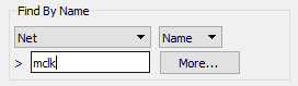
Then press either the Tab, or Enter key, the screen will zoom to the ratsnest area and the ratsnest line for the MCLK signal will be displayed.
Look at the ratsnest for the MCLK net.
7. Right-click>Done in the canvas background to end the Show Rats command
8. Left-click the Add Connect icon  (or Route>Connect from the menu or F3 if using default function keys)
9. Left-click Options, before you select a connection to start routing, the settings should match the following illustration:
(Active: Top, Alternate: Bottom)
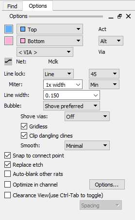
10. Left-click on the pin of the J1 connector, which is the endpoint of the MCLK ratsnest line.
11. Move the mouse away from the pin and see that the route appears, left-click will accept the current routing as you proceed. Notice also that the net name and the correct line width for MCLK are now displayed in Options when visible. You can change the Line Lock angle in Options to 45 after starting to add the routing.
12. Continue to left-click points for the line until you reach the destination pin, similar to the following figure:
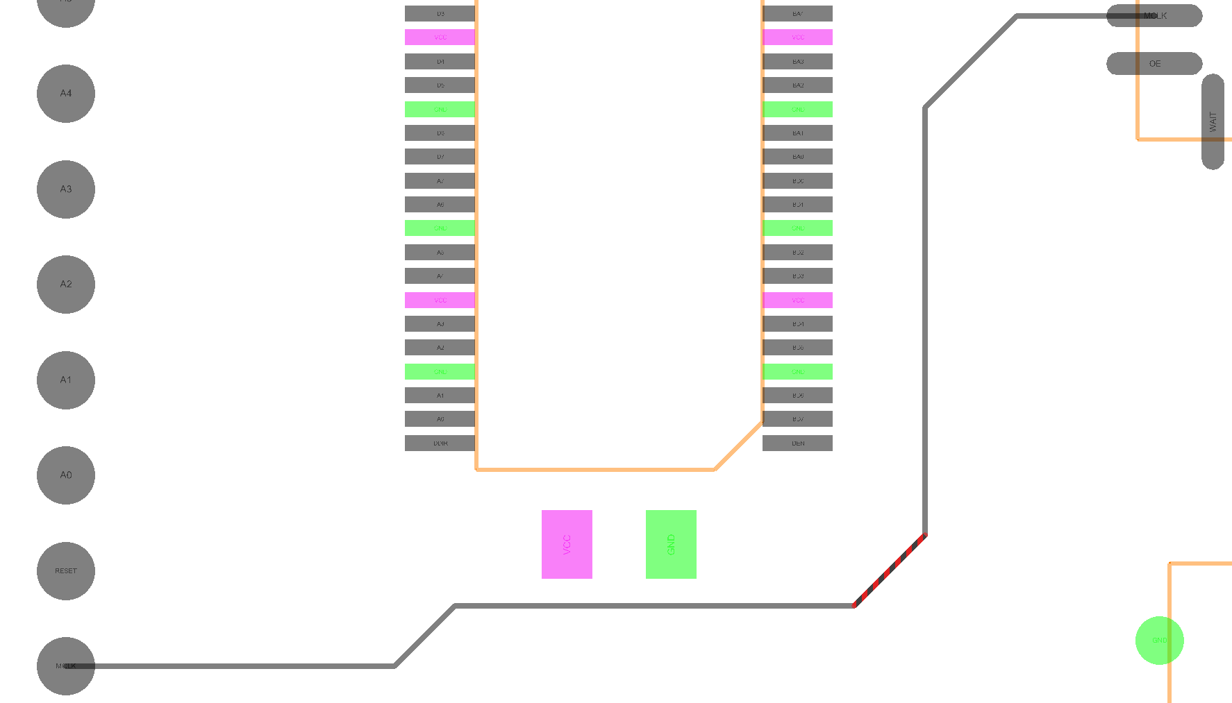
If you make mistakes while picking points, right-click>Oops to undo the last step, this can be repeated, if necessary to remove multiple sections.
When you reach the destination pin, the ratsnest line disappears, denoting the completion of that connection.
13. Right-click>Done from the pop-up menu
14. Left-click the Delete icon  in the toolbar.
15. Left-click Find to activate it
16. Left-click>All Off
17. Check the Clines (connect lines) box to ON in the Find window.
18. Left-click on the routed MCLK in the canvas.
The connection becomes highlighted.
19. Right-click>Done to confirm Delete
20. Select Setup>Application Mode>Etch Edit
21. Move the mouse into the canvas background and right-click>Customize>Enable Single Click Execution. It this option is already checked, do NOT uncheck this option.
22. Move the mouse to the Find Filter and left-click the All On button.
23. Left-click on the J1 pin of the MCLK net.
PCB Editor enters the Add Connect command.
24. Use left-clicks again to add the routing to the destination pin.
Once the destination pin is clicked, the connection is made to the pin and the Add Connect command is ended.
25. Move your cursor over one of the horizontal pieces of etch. A datatip should be displayed stating Horizontal line segment, net MCLK, Etch class, subclass Top.
26. Select right-click>Delete from the pop-up menu.
27. Move your cursor over another piece of the etch for the MCLK net.
28. Press the Tab key until the datatip shows “Net”for MCLK.
29. Right-click and select Ripup Etch from the pop-up menu.
This deletes all of the remaining etch on the Top layer for the MCLK net.
30. Left-click in the canvas background to clear any selections and then left-click the Add Connect icon in the toolbar.
31. Left-click Options to activate the tab
32. In Options, check / set the Active: Top and Alternate: Bottom as shown:
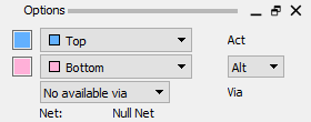
33. Left-click on the pin of the MCLK net in the J1 connector, the pin connected to one end of the ratsnest.
34. Once again, begin adding segments from that pin toward its destination.
35. When you have reached a point where you would like to add a via, double-click. See the figure.
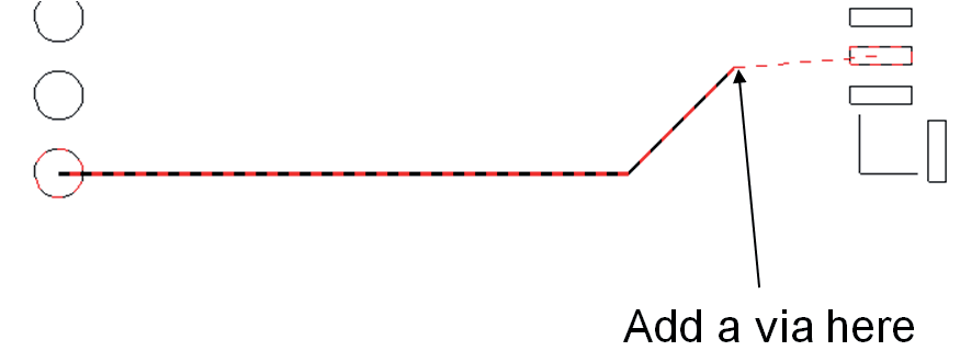
You have just added a via, and the Active and Alternate layers in the Options window have been swapped. You are now adding on the BOTTOM layer.
36. Finish the connection all the way to the pin of the U5 component.
Since the destination pin is on a surface-mount device on the top side of the design, add another via to finish the route on the TOP layer.
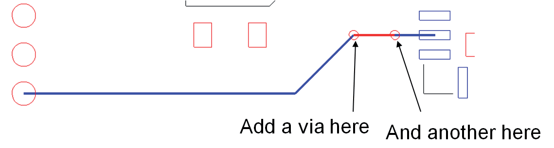
37. Right-click>Done from the pop-up menu.
Look at how the connection you just added uses two different etch layers with routing vias.
38. Left-click the Rats All icon to turn on all ratsnests. Zoom into an area to view one end of a ratsnest on the pin just below the MCLK pin of the J1 connector, and the other ratsnest connection on the U5 component in view. See the following figure.
Note
Your view may differ slightly, depending on how your components are placed.
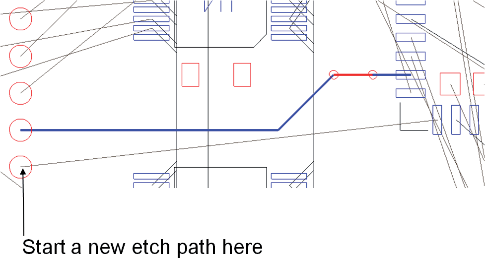
39. Left-click the Add Connect toolbar icon.
40. Activate Options, select Shove Preferred in the drop-down and, under Smooth, set the option to Full.
41. Click on the pin just below the MCLK pin of the J1 connector. This is the WAIT net.
See the previous figure.
Check Options for the active layer set to TOP.
42. Start moving your cursor toward the existing etch of the MCLK net. The existing etch will be “shoved”, or moved, as the new etch becomes closer than the DRC “line to line” value.
43. Experiment with the different Smooth Options of Off, Minimal, Full and Super Smooth that are available, and with the different Bubble Options of Off and Hug Preferred. Also experiment with the Shove vias Option.
While you are in this mode, there may be some instances when the trace to be added will create a DRC, when this happens, your cursor will change to a DRC marker. (“bow tie”)
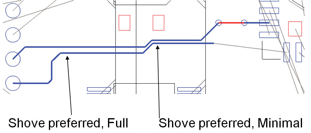
44. Finish routing the WAIT net.
45. Right-click>Done
46. Select File>Save As from the top menu.
47. In the File Name field, enter:
b4route
48. Left-click>Save.
The file b4route.brd has been saved to disk. You now have three options in regard to routing:-
- Manually finish routing this design to completion using the steps you have learned in this lab. Once complete move onto Lab 12-5.
- Take this design and follow the steps in Lab 12-3 which will route the design using an alternative routing method called Working Layer. You will add some additional routing layers to help with this process and complete routing the design using both this method and the steps above. Then move to Lab 12-5.
- Take this design and follow the steps in Lab 12-4 and use the auto-router to route the board. Then move to Lab 12-5.
- Move straight onto Lab 12-5 using a pre-routed design called routed.brd. This design was autorouted using an OrCAD PCB Designer Professional License. (Steps for the autoroute process can be found in Lab 12-4)
End of Lab
All content Copyright 2022 Parallel Systems Ltd.