
3D View
The 3D view is not essential to designing the board but it does give an idea of what the board will look like based upon the STEP models mapped to the Package Symbols and can be useful in discussions about details of the “finished” board. It can also give early indication of incorrect models / footprint clashes with other parts and enclosures or mechanical parts. For the lab data, all of the Package Symbols have STEP models attached. Some have been created by library tools and some have been downloaded from the internet – these can usually be identified because the lead lengths are defined from the original datasheet and not “trimmed” to the board thickness.
The 3D view will display what is selected in the PCB Editor canvas so it is possible to view the entire board, or a selection of Nets and / or Package Symbols from the board.
If an STEP model enclosure is imported into the Board, the 3D view can display clashes between the enclosure and components, as well as component to component.
Reference Designator rename
When the schematic is drawn, it is unlikely that any consideration is given to the final, physical, layout of the board. As a consequence, the Reference Designators, which might be “orderly” in the schematic, will become “distributed” around the finished board. For some users this isn’t a particular problem because there may be little need for any board repair at a remote location and the availability of the board data, or the board Assembly Drawing exported to PDF, to view for any servicing, or repairing, might be satisfactory. For other users, having the Reference Designators “ordered” on the board can aid in locating components when servicing, or repairing, the board. PCB Editor can rename the Reference Designators, and reorder them, through the Reference Designator Rename processing. Since some discrete components can share footprints, it is essential that the “Preserve Current Prefixes” option is checked, otherwise, the Reference Designator placeholder text from the original Package Symbol will be used – the Package Symbols in the lab design all have “REF” as the Reference Designator placeholder so the majority of the references will become “RE<some number>” if the “Preserve Current Prefixes” is not checked for this process in the lab.
In PCB Editor, the only place that the Reference Designator value is held is the text itself, so, individual components can have their Reference Designator value changed by “simply” editing the Text value. Note that, if the Reference Designator value is changed to a value that already exists on another component in the design, the Reference Designator values will be exchanged.
Design Sync between board and Schematic
Changes made in the PCB need to be synchronised with the Schematic otherwise loading an updated netlist can result in those changes being undone. The Design Sync process in Capture is started from either PCB>Update Layout, to update the board from the schematic, or PCB>Update Schematic, to update the schematic from the board. During this Design Sync process, the “current state” of the Schematic and the “current state” of the Board will be compared and changes applied to the board or schematic depending on which Update was selected. The Design Sync process synchronises any Pin and Gate (Function) swaps, Reference Designator changes and Part and Net Properties from the Board to the Schematic. It will also import any of the data from Constraint Manager if this flow has been enabled, so Electrical, Physical, Spacing and Same Net Spacing constraints can updated to the Schematic.
Silkscreens
Silkscreen is added to the board to provide Reference Designator text, and orientation details, to identify components for assembly and test. Since many products are now automatically assembled and tested, and have little “free” space to place the text, the practice of providing Reference Designator text on PCBs has declined somewhat. Strictly speaking, the Silkscreen is the pattern that is used to deposit the “ink” that forms the Reference Designator text, and other details, on the PCB but this term is often used to refer to the details that are left by the silkscreen processing.
When the Package Symbols get created, there can be no knowledge of the details of the board that they will be placed in so, any silkscreen details added at that point may conflict with other objects (such as pins or vias) in the design once the components are placed and the design routed. The silkscreen details in the board could be moved manually to remove any conflicts with other objects but PCB Editor provides assistance through the Manufacture>Silkscreen process which allows selection of which silkscreen objects and subclasses are processed. During the silkscreen processing, Lines, if selected, will be cut and Text, if selected, will be moved (since cutting text is likely to make it unreadable) and copied to an Autosilk layer. Text and lines on the Autosilk layers can then be manually edited, if required, without affecting the original Package silkscreen details.
Reports
In PCB Editor, the Export>Reports and Export>Quick Reports menus provide access to reports. The reports provided by both menus are the same but the Export>Reports menu allows multiple reports to be selected and also allows custom reports to be created, whereas the Export>Quick Reports menu only allows a single report to be selected. Reports are displayed after creation and can then be saved from the displayed window.
Drafting Utilities Overview
The Drafting commands functionality is designed to improve the user’s experience editing, deleting and creating various drafting information on the canvas. Users should note that although intended for drafting content, all of these commands will also act on conductor subclasses in addition to documentation subclasses.
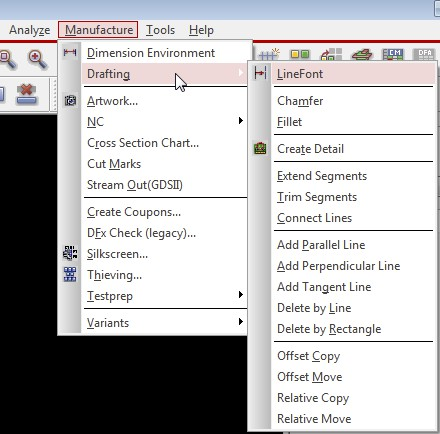
• Extend and Trim Segments
• Connect Lines
• Add Parallel, Perpendicular and Tangent Line
• Delete by Line and Rectangle
• Offset Copy and Move
• Relative Copy and Move
The commands are located in the Manufacture>Drafting menu.
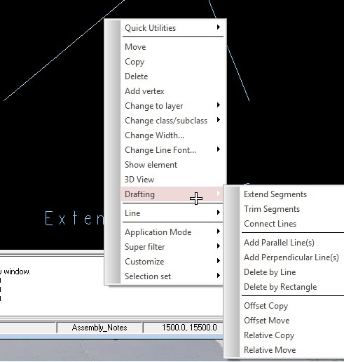
They are also available on the context sensitive menu when in General Edit Application Mode.
(e.g. RMB-Drafting on a “line”)
All content Copyright 2022 Parallel Systems Ltd.