
All content Copyright 2022 Parallel Systems Ltd.
1. With the schematic page still open from the preceding labs, press Control+left-click to select both the 74F162 and 74LS00 parts.
2. Right-click and select Edit Properties.
Observe that the properties for both parts are displayed in the Property Editor window.
3. Left-click in the PCB Footprint field for the 74LS00 part and enter:
DIP14
a. Left-click>Apply to set the value.
b. Left-click>Display
c. Set the Display Format to Value Only and left-click>OK.
This makes the value of the PCB Footprint property visible in the schematic.
4. Left-click in the PART_NUMBER field for the 74LS00 part and enter:
20-12345
5. Left-click>Apply to set the value.
6. Left-click in the PCB Footprint field for the 74F162 part and enter:
SOIC16
7. Left-click>Apply to set the value.
8. Close the Property Editor tab.
9. Press Esc to deselect both parts.
10. Select both the 74F162 and 74LS00 parts again.
11. Press Control+E to display the Property Editor. (Or right-click>Edit Properties)
12. Left-click on the PCB Footprint property name box on the left (as shown in the following graphic).
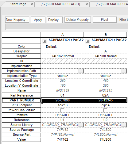
All PCB Footprint property values are highlighted.
13. Left-click>Display.
a. In the Display Properties window, choose Do Not Display.
b. Left-click>OK.
14. Close the Property Editor and press Esc to deselect all parts.
Observe that all PCB Footprint properties are now invisible.
15. Select both the 74F162 and 74LS00 parts again.
16. Right-click>Edit Properties (or press Control+E).
17. At the top of the Property Editor window, left-click>New Property.
The Add New Property window appears.
18. In the Name field, enter:
VENDOR
19. Left-click>OK.
The VENDOR property is added to the Property Editor
20. Left-click the VENDOR property name box (on the left).
21. Right-click>Edit from the pop-up menu.
The Edit Property Values window displays.
a. Left-click in the VENDOR field and enter:
Jumbo Parts
b. Left-click>OK.
The VENDOR name is applied to both parts.
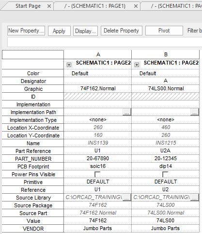
22. Close the Property Editor and press Esc to deselect all parts.
Note
You can also use the Control+C and Control+V keys to copy and paste property values between cells in the Property Editor window.
23. Go to Edit>Find, or press control+F to activate the Find pane.
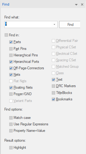
24. Enable the check boxes for Nets (only for Find In) and Highlight and check that * is in the “Find What:” box.
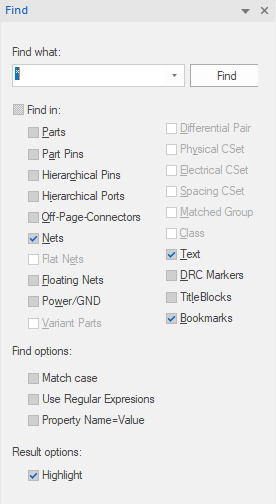
25. Left-click>Find to perform the search
The Find results pane opens and the Nets are highlighted in the Schematic Page
26. Hover the mouse over the selected Nets in the Schematic Page and right-click>Edit Properties within the schematic page.
Note
The following exercise illustrates adding a property to a wire. The override Property for width in PCB Editor is MIN_LINE_WIDTH. This property was added to the LOAD Net in the previous lab, if the property isn’t listed, use the New Property button to add it.
27. Left-click in the MIN_LINE_WIDTH name cell on the left to select the row, then right-click>Edit
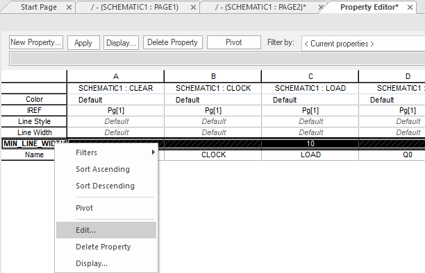
28. The Edit Property Values box opens, the only action is to type in the box, so just type a value, 10 in this case.
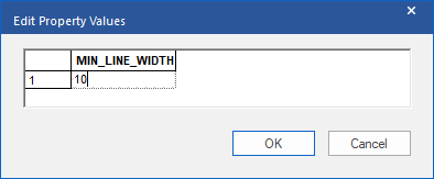
29. Left-click>OK
The MIN_LINE_WIDTH value of 10 is assigned to all Nets.
30. Close the Property Editor and press Esc to deselect all nets.
31. Left-click the “X” to close the Search Results pane.
32. Select File>Save and left-click>OK to save all pages of the design.
33. Close the schematic page.
End of Lab
All content Copyright 2022 Parallel Systems Ltd.