
All content Copyright 2022 Parallel Systems Ltd.
1. In the Release Root Schematic folder, double-click on PAGE1.
2. If necessary, enlarge the schematic window, and zoom to fit.
3. Locate the 64-pin connector (J?) along the left side of the page.
Observe that pins 1, 2, 3, and 33 are not connected.
4. There are several GND symbols already on this page, Copy one of them, and place it slightly to the right, centre of the J1 connector, as shown in the following graphic near pin 33.
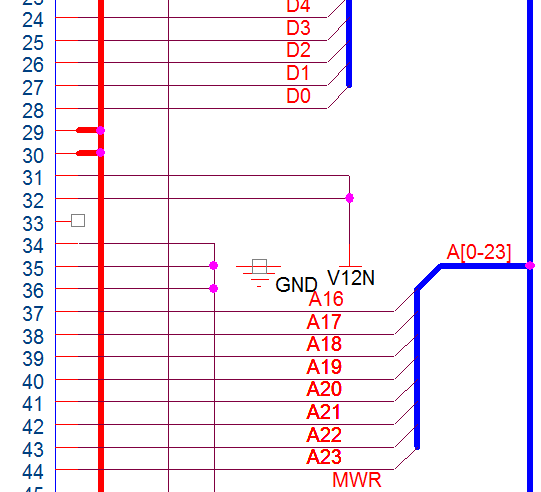
5. Left-click the Place wire icon, or press W.
6. Connect pins 1 and 33 to the GND symbol you placed in step 2.
If necessary, use the <I>, <O>, and <C> keys to zoom in or out and pan while adding the wire.
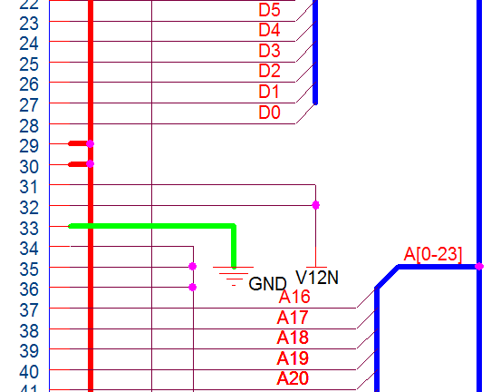
Notice that when you connect a pin, the unconnected box at the end of the pin disappears.
7. Draw wires from pins 2 and 3 as shown in the graphic below.
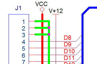
When a connection between two wires is made, a junction dot appears at the intersection.
8. Press Esc twice.
9. Save the design.
The Release Root Schematic, PAGE1 contains six FCT16245 parts as shown in the graphic below. Three of these parts are missing connections.
In this lab the a BA[0-7] bus will be added to the three parts shown below.
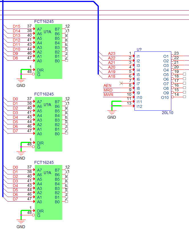
The graphic that follows shows the BA[0-7] bus you will be adding as you complete this lab. Your schematic should match this schematic after you complete this section of this lab.
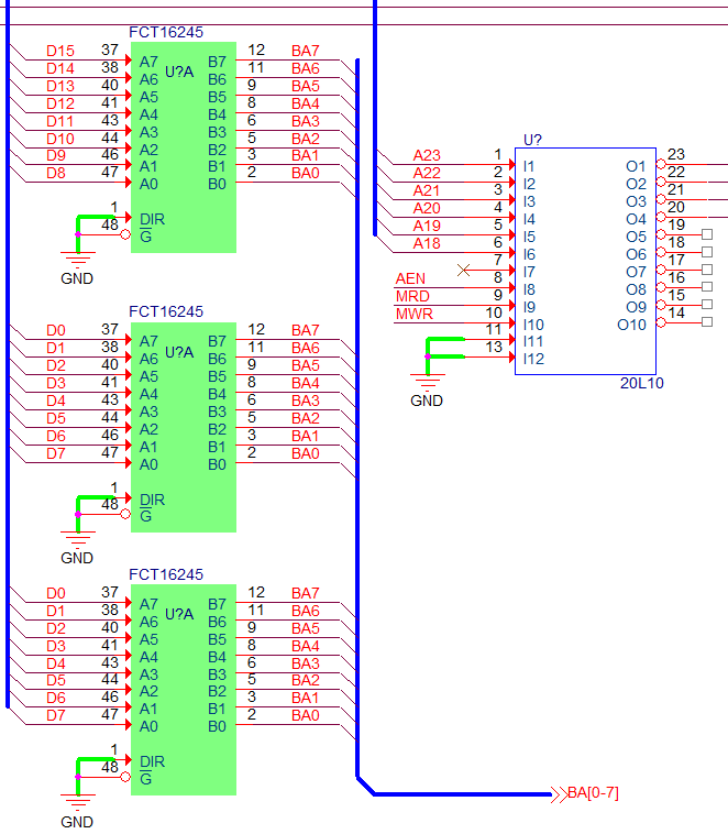
10. Starting with one of the FCT16245 parts, add a wire segment to pin 12.
11. Then press F4 to replicate the segment for the other 7 wires, as shown in the following graphic.
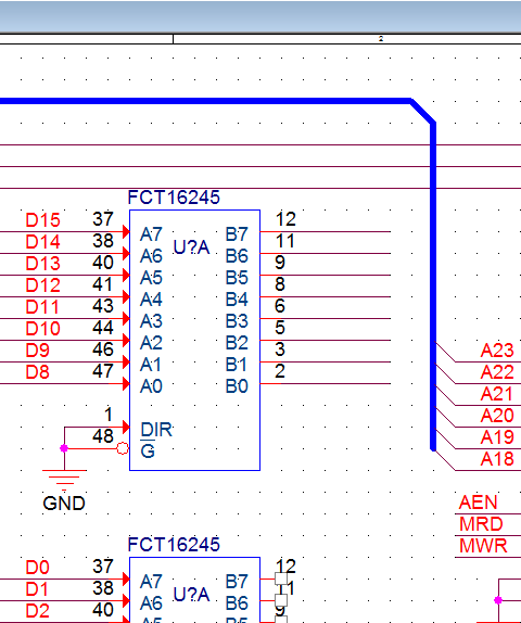
12. Press Esc twice.
13. Select Place>Net Alias, or press the N key, name the alias, BA0, and left-click>OK and left-click on the bottom wire connected to pin 2.
14. Move the mouse up to the other wires and left-click each wire to place the aliases.
The alias automatically increments from the starting number, BA0, to BA7, as shown in the next graphic.
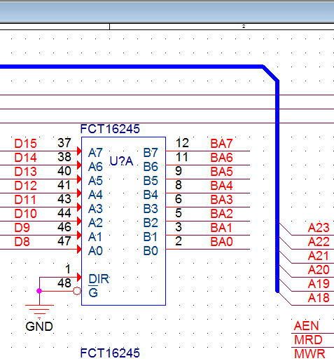
15. Press Esc twice.
16. Place a bus entry on the BA7 wire. If necessary, use the R key to rotate it before placing (as shown in the next graphic).
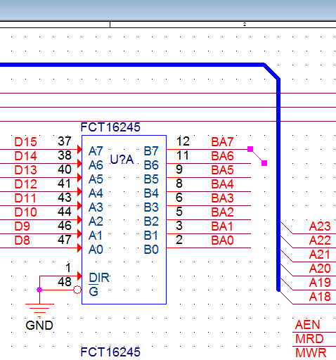
17. Press the Esc key once, then press the F4 key seven times to replicate the bus entry on wires BA6 through BA0.
18. Press Esc to exit the command.
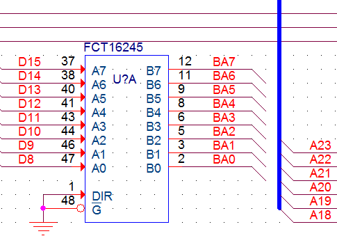
19. Drag a rectangle around the new connections, right-click, and select Copy from the pop-up menu (or Control +C).
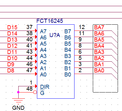
20. Press Esc to deselect, then right-click>Paste (or Control+V).
21. Place copies of these connections on the other two FCT16245 parts.
Caution
If you have Options>Preferences>Select, Intersecting enabled, be sure the rectangle does not touch any pins on the part, or they will be selected also. (The Fully Enclosed selection option maybe useful in these kinds of situations.)
22. Save the design.
23. Left-click the Place bus icon or select Place>Bus from the top menu.
24. Left-click to start drawing the bus, starting at the top of the page is probably easier. End the bus with a double-click and hold the Shift key to draw the angled corner, if required. Refer to the graphic earlier (step 9) for the desired result.
Note that the bus will work with a simple right-angle.
25. Left-click the Place off-page connector icon or select Place>Off Page Connector from the top menu.
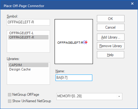
The Place Off-Page Connector form appears.
26. In the Libraries list, check that CAPSYM is in the selected libraries, blue background, list, left-click on the CAPSYM entry if it is not one of the selected libraries.
27. From the Symbol list, select OFFPAGELEFT-R.
28. In the Name field, enter BA[0-7] and left-click>OK.
29. Place the Off-page Connector in the schematic page and press R twice to rotate the
symbol to “point” right. (“Before” and “After” in the next shot)
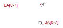
30. Move the Off-page Connector symbol and attach it to the end of the bus wire.
31. Left-click in the schematic page, or press Esc to deselect the Off-page Connector.
32. Save the design.
Note
You can also place the generic off-page connector and edit the name at a later time. Both ways are correct. The Off-Page Connector will need to have a Bus Name specified to attach to a bus.
Now place the remaining off-page connectors.
33. Locate the 20L10 part, upper right corner of the page.
34. Use this example and the following steps to add the Off-page Connector to the pins on this part.
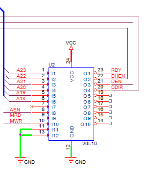
35. Again, choose the Place Off-Page Connector icon, or select Place>Off-Page Connector from the menu.
36. In the Place Off-Page Connector window, select OFFPAGELEFT-R from the CAPSYM library.
37. In the Name field, enter:
HS/
38. Left-click>OK.
The connector is pointing left.
39. Press R twice to rotate it to point right.
Caution
Beware of “special characters”. Some netlisters for other board layout tools will not accept them. For PCB Editor the only ones to avoid are “!”, “, ‘ and space.
40. Place the symbol on pin 19 of the 20L10 part and then drag the Off-Page Connector a couple of grids to get a wire added.
41. Check the Online DRCs window. There is a message that flags “HS/” has “less than two connections”. Scrolling through the Online DRCs there is another message that flags “HS” as having “less than two connections”.
Since “any” design might be in the process of being completed, these messages might be perfectly reasonable at this stage but, in this case, the correct name for this Off-Page Connector is “HS” so, double-click on the “HS/” text, change it to “HS” and left-click>OK to apply the change.
Note
If you place the symbol directly on the pin, a connection is automatically created between the pin and the off-page connector. However, if you intend to place properties on the net you must have a wire segment. Properties are placed on Parts and Wires. If you move the off-page connector, a wire will appear connecting it to the pin.
42. Repeat this operation to place five more Off-page Connectors.
After placing each connector, press control+E, or right-click>Edit Properties, and use the Edit Off-Page Connector window to specify the name of the next connector to be placed. Assign the names HS, FPGA, BWR, BRD, BRESET, SEL from top to bottom, Pin 19 down to Pin 14.
43. Again drag the Off-page Connectors away from the Pins by a couple of grids to get a short wire segment added between the Pin and the Off-page Connector.
44. Save the design.
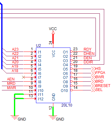
45. Zoom into the area, towards the middle bottom of the page, as shown in the following screen shot.
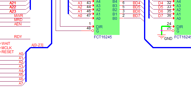
46. Left-click the Place part icon or use Place>part from the top menu.
47. In the Libraries list, left-click on Design Cache, double-click on the CAP NP entry from the Part List to get the part onto the cursor.
DO NOT place the part yet.
48. Move the mouse into the schematic page and right-click>Edit Properties.
a. In the Value field, enter:
0.1uF
b. In the PCB Footprint field, enter:
SM_1206
49. Left-click>OK.
50. Place four capacitors, as shown in the following graphic.
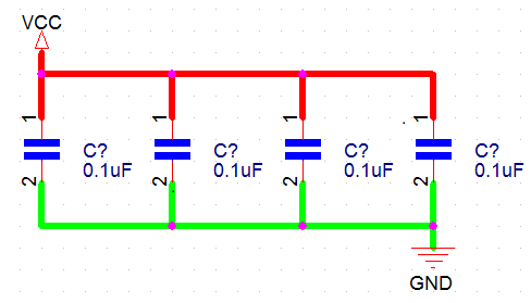
51. Press Esc twice.
52. Add wires, as shown in the example on the previous page.
53. Copy existing VCC and GND symbols and complete the circuit.
54. Save the design.
55. Go to the Project Manager window, and in the Release Root Schematic folder, double-click on PAGE2.
56. Zoom into the area near the top of the page where the FPGA and Net Group are, see following graphic:
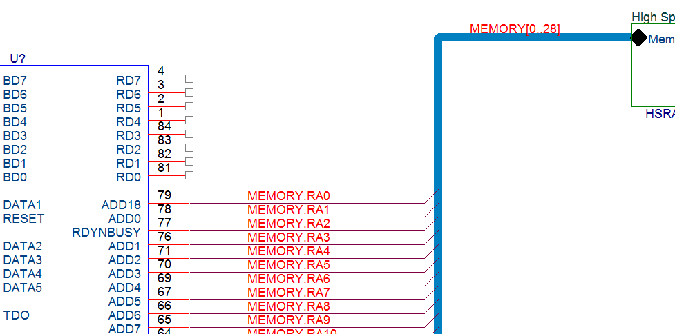
57. Select the 8 data unconnected pins at the top of the FPGA, either with a window select around the pins or a control+left-click on each of the pins.
58. Hover the mouse over one of the selected items to get a “4-pointed” cursor for the mouse, then right-click>Connect to Bus, the cursor will change to a “diagonal” cross, then left-click on the NetGroup. (Wide Blue Bus labelled MEMORY[0..28])
59. The Select Nets dialog will open, left-click on the + to the left of Memory to expand the NetGroup members and then left-click in the checkbox for Memory:RD[0..7] to select these nets.
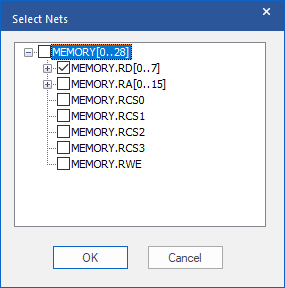
60. Left-click>OK to get the net names applied.
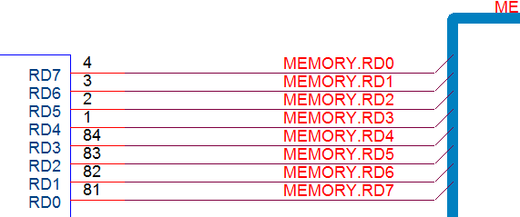
The net names are applied top to bottom in the order from the range specified in the NetGroup definition, in this case, 0, 1, to 7. This does not match the pin naming of the FPGA pins but this will not affect functionality. (You can move the Net Aliases to re-order them if you wish to get the Net Names and Pin Names to align)
61. Use File>Save to save the changes to Page2.
62. Go back to the Project Manager window, and double-click PAGE1 in the Release Root Schematic folder, to open it.
(Or select the Page1 tab if the page is already open)
63. Locate the 20L10 part in the upper right corner of the page and double-click on it to open the Property Editor.
64. Locate the Power Pins Visible property.
65. Left-click the Power Pins Visible checkbox, as shown in the graphic that follows.
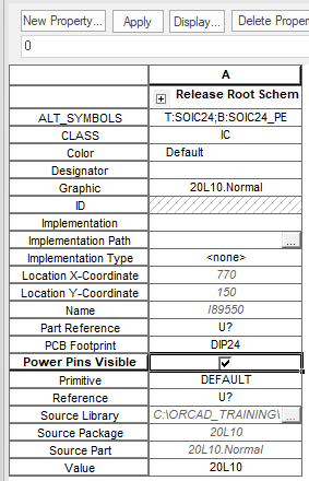
66. Close the Property Editor window.
67. Press Esc, and zoom in to view the part.
The power pins on the 20L10 part are now visible (top and bottom).
68. Copy a VCC symbol and connect it to pin 24 (at the top of the 20L10 part).
69. Copy a GND symbol and connect it to pin 12.
Check that you have a short piece of wire between the Pin and both Symbols
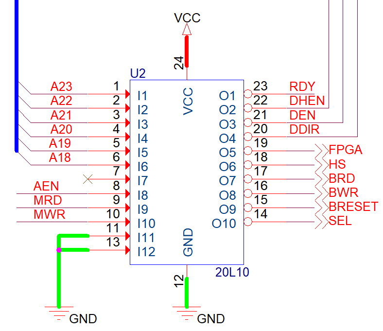
This screen shot shows a “vcc_arrow” symbol, you may have a “vcc_circle” in the schematic page, this doesn’t matter provided that the symbol name is “vcc” to get the correct net name.
70. Select File>Save to save the schematic page.
Note that there are no Online DRCs listed now.
71. Select File>Close to close the schematic window.
72. Leave this project open for the next lab.

End of Lab
All content Copyright 2022 Parallel Systems Ltd.