
All content Copyright 2022 Parallel Systems Ltd.
Note
If an existing schematic is already part of the Design Folder and has hierarchical ports for inputs and outputs, when the hierarchical block is created referencing that schematic, Capture automatically places the appropriate pins on the block symbol as demonstrated in previous lab exercises.
Note
If you want to create the hierarchical block first and create a schematic view later, the block must be drawn manually.
Note
In this supplemental lab exercise, the hierarchical block will be manually built in the Data schematic as shown in the graphic below.
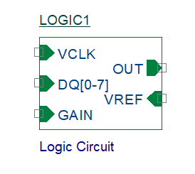
1. In the Project Manager, double-click on Page1 of the Data Schematic to open the page.
2. Left-click in the Data schematic window, and select the Place hierarchical block icon or select Place>Hierarchical Block from the top menu.
3. In the Reference field, enter:
LOGIC1
4. Set the Implementation Type to Schematic View.
5. In the Implementation name field, enter:
Logic Circuit
6. Left-click>OK.
7. In the lower left corner of the page, drag a rectangle to define a hierarchical block symbol.
8. Press Esc.
Because there is no LOGIC CIRCUIT schematic yet, the hierarchical block you draw does not have pins created automatically, as occurred in the previous exercise.
9. Left-click on the LOGIC Circuit block symbol to select it, and left-click the Place pin icon, or use Place>Hierarchical Pin from the menu.
The Place Hierarchical Pin window displays.
10. In the Name field, enter:
DQ[0-7]
Set the Width to Bus and set the Type field to Input and left-click>OK.
A hierarchical pin attaches to the edge of the rectangle. As you move your cursor, the block pin moves along the perimeter of the rectangle.
11. Left-click to place the pin along the left edge of the rectangle, near the lower left corner.
12. While in add pin mode, right-click>Edit Properties.
13. In the Place Hierarchical Pin window, change the Name field to GAIN, the Width to Scalar and left-click>OK.
14. Add a GAIN pin two grids below pin DQ[0-7].
15. Add a VCLK pin two grids above pin DQ[0-7].
16. Add a VREF pin on the right edge of the rectangle.
17. Before adding the next pin, right-click>Edit Properties.
18. Change the Name field to OUT.
19. Set the Type field to Output and left-click>OK.
20. Add the OUT pin below the VREF pin.
21. Press Esc twice.
22. Save the design.
23. Left-click on the LOGIC Circuit block to select it and right-click>Descend Hierarchy.
Capture prompts you for the name of the new schematic page for the Logic Circuit.
24. Left-click>OK to accept the Page1 default.
The LOGIC CIRCUIT schematic window opens. Observe how Capture automatically added hierarchical port symbols to the new schematic page. These ports correspond to the pins added to the block.
25. Save the design and close both the LOGIC CIRCUIT and Data Schematic pages.
26. In the Project Manager window, observe that a new schematic folder was added for the LOGIC CIRCUIT.
The LOGIC CIRCUIT block symbol and its associated schematic have been left unconnected. These errors would be flagged by the DRC process.
As we will not be using this block symbol in the next labs, remove it from your schematic page. Also, go to the Project Manager and delete the new schematic folder. Remember to save your design.

End of Lab
All content Copyright 2022 Parallel Systems Ltd.