
All content Copyright 2022 Parallel Systems Ltd.
As far a practicable, the schematic should be completed before adding the Constraints.
Example 1: With a completed Schematic only
1. Start OrCAD Capture with an OrCAD PCB Designer Professional, or start OrCAD Capture CIS with an OrCAD Capture CIS license.
(If you start with an OrCAD Capture, or an OrCAD Capture PCB Designer Standard, license, only a limited number of Electrical Constraints will be available)
2. Use File>Open>Design and open the Release.dsn file from the C:\OrCAD_Training\Capture\CMLabs\Example1 directory.
3. Use File>Save to save the Project file.
(If you have the Online DRCs tab active, ignore the warnings about “missing footprints”, these will be resolved once the schematic has been coupled with a board and the board location has been defined)
4. Use PCB>Constraint Manager or left-click the Constraint Manger toolbar button.
5. Left-click>OK on the Enable Constraint Manager form
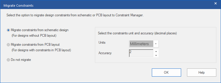
6. On the Migrate Constraints form, check that the “Migrate Constraints from Schematic Design” is selected. Set the Units to “Millimeters” and Accuracy of 2 Decimal Places.
7. Left-click>OK
8. The “Assign Voltage to Power Nets” form is shown.
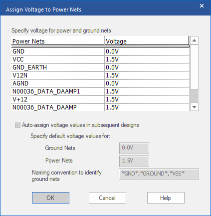
Accept the defaults, or assign other voltage values.
(The Auto Assign, if set, will apply to any additional designs that are opened in the same session and converted to Constraint Manager enabled)
9. Left-click>OK to close the form.
10. Activate the Constraint Manager window, from the Capture icon in the Windows Task Bar, from the PCB>Constraint Manager menu, or from the Constraint Manager icon.
The Domains, Electrical, Physical, Spacing, Same Net Spacing and Properties, are shown at the left.
If the Physical Domain is active, note that, in the Physical Constraint Set>All Layers, all of the values have a hatched background because the rules are layer specific and there is currently no cross-section loaded to define any layers.
(A schematic doesn’t have / need a cross-section)
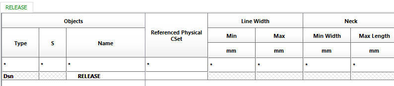
(This also apples to the Spacing and Same Net Spacing Domains which are layer specific as well)
Rules at this point can be applied directly to Nets and any values will be applied to all layers when a netlist is created and loaded into a board.
It is possible to get a “default”, two layer, cross-section using the following steps:
(Note that the library files for the PCB Footprints will be required for this process)
11. Use File>Close to close the Constraint Manager window
12. In the Capture window, left-click the Release.dsn file entry in the Project Manager
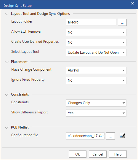
13. Start PCB>Design Sync Setup
14. Set Select Layout Tool to “Update Layout and do not open”
15. Left-click>OK
16. Start PCB>New Layout
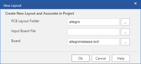
17. Left-click>OK
(Yes / OK any messages from the Create Netlist processing)
18. Left-click the “X” in the upper right of the Constraint Difference Report to close it.
19. Start PCB>Update Schematic
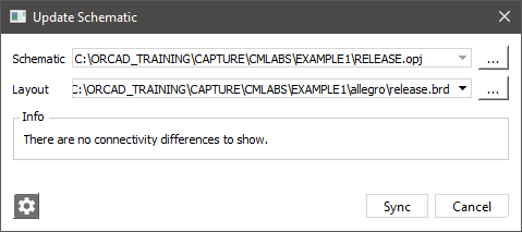
20. Left-click>Sync
21. Left-click the “X” in the upper right of the Constraint Difference Report if it appears.
22. Use PCB>Constraint Manager, or the CM icon from the toolbar, to activate the Constraint Manager window again.
23. Left-click>OK on the “Migrate Constraints” message
24. Go to the Physical Domain, then Physical Constraint Set, All Layers, “open” the Default Constraint Set and note that the layers, and default values have been imported.
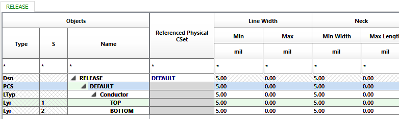
Things to note:
1) The board file default settings for Units and Accuracy will override those set in Capture.
2) A complete set of footprint libraries is required for the schematic to be able to create a netlist and update a board
3) Once the design has been enabled for the Constraint Manager flow, it cannot be reverted.
4) Renaming any of the sub folders of the schematic will also cause the constraints to be removed from the DSN file.
Example 2: With a completed Schematic and an existing board
1. Start OrCAD Capture with an OrCAD PCB Designer Professional, or start OrCAD Capture CIS with an OrCAD Capture CIS license.
(If you start with an OrCAD Capture, or an OrCAD Capture PCB Designer Standard, license, only a limited number of Electrical Constraints will be available)
2. Use File>Open>Design and open the Release.dsn file from the C:\OrCAD_Training\Capture\CMLabs\Example2 directory.
3. Left-click>OK in Select Project Type
(Don’t enable PSpice Simulation)
(Again, ignore the warnings about the “missing footprints”)
4. Use PCB>Constraint Manager or left-click the Constraint Manger icon.
5. Left-click>OK on the Enable Constraint Manager form
6. On the Migrate Constraints form, check that the “Migrate Constraints from PCB Layout” is checked and left-click>OK
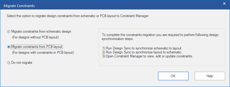
7. The actions listed on the right need to be completed so, left-click>OK
8. The “Assign Voltage to Power Nets” form is shown. Accept the defaults, or assign other voltage values.
(The Auto Assign, if set, will apply to any additional designs that are opened in the same session and converted to Constraint Manager enabled)
9. Left-click>OK to close the form.
10. In the Capture window, left-click the Release.dsn file entry in the Project Manager
11. Start PCB>PCB Design Sync Setup
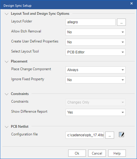
12. Check that Select Layout Tool is set to PCB Editor and left-click>OK
13. Start PCB>Design Sync
14. Set the New Layout form to match the settings below:
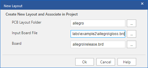
Note: The Input Board File path has been edited to fit in the form.
Left-click the “…” to the right of “Input Board File” to browse for the input board, the path should be C:\OrCAD_Training\Capture\CMLabs\Example2\allegro\gloss.brd
15. Left-click>OK
16. The Constraint Differences Report opens and there is a prompt to choose a PCB Editor license to open the Board, select any valid license and left-click>OK to start PCB Editor with the release.brd open.
17. Use File>Save As in the PCB Editor window and overwrite the release.brd file
(Just to ensure that everything is up to date)
18. Back in the Capture window, start PCB>Update Schematic
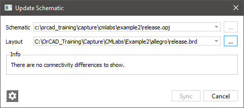
19. Left-click>Sync
20. Close any Constraint Difference Report windows that may be open.
Note that, once the board has been created, the Online DRCs are no longer reporting “missing footprints”
21. Start Constraint Manager
21. Left-click>OK on the “Migrate Constraints” message
22. Go to the Physical Domain, then Physical Constraint Set, All Layers, open the Default Constraint Set and note that the layers, and values have been imported from the board.
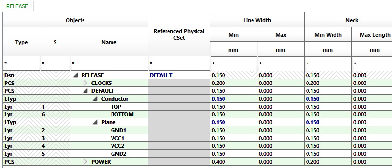
This board is an active design so, since the Schematic had no design rules, all of the rules from the board have been imported.

End of Lab
All content Copyright 2022 Parallel Systems Ltd.